LED Tungsten Copper Heat Base and Other Materials Comparison
- Details
- Category: Tungsten Information
- Published on Wednesday, 29 June 2016 14:28
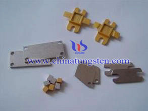
Most of LED products, usually you need more than one LED assembled on a circuit board. The circuit board not only needs to carry LED module structure, but also plays an important role in heat dissipation. LED heat dissipation board consists of two major components, one is the system board, and the other is LED grain substrate. Most of the system board is made of metal, which takes advantages of excellent heat dissipation characteristics of its own to achieve the effect. However, with the increasing brightness and efficacy requirements of LED, the bottleneck will appear on the LED grain substrate. In order to break the bottleneck of heat dissipation, researchers around the world look for and develop the substrate materials with high thermal coefficient. Currently, several common LED heat dissipation substrates comprises rigid printed circuit boards, high thermal conductivity aluminum plate, a ceramic substrate, soft printed circuit boards, metal composite materials.
Tungsten copper board for heat dissipation is currently recognized as the most performance fit a class of materials. It has many advantages, such as high strength, low coefficient of thermal expansion, high heat transfer coefficient and so on. By adjusting the component can make up a single hot metal chips and LED mismatch insufficient, so it has been widely used in some large scale integrated circuits, high-power devices, as the radiating element. In addition, electrolytic polishing tungsten copper foil surface finishing can effectively improve the heat dissipation of tungsten copper LED substrate surface flatness to meet the stringent requirements for heat dissipation board of flatness. Thick film ceramic substrate fabricated by screen printing technology and with a spatula printed material on the substrate, after drying, sintering, laser and other processes. But with the decreasing size and lines of LED, higher requirements for precision, the accuracy of such board has been unable to reach. Low-temperature co-sintered multi-layer ceramic substrate printed on the board by screen printing and then integrating the multilayer ceramic substrate, and finally through the low-temperature sintering. But it is supposed to consider the shrinkage ratio after multi-layer ceramic sintering, which is difficult to be controlled.
| Tungsten Copper Supplier: Chinatungsten Online tungsten-copper.com | Tel.: 86 592 5129696; Fax: 86 592 5129797;Email:sales@chinatungsten.com |
| Tungsten News & Prices, 3G Version: http://3g.chinatungsten.com | Molybdenum News & Molybdenum Price: http://news.molybdenum.com.cn |
LED Tungsten Copper Heat Base
- Details
- Category: Tungsten Information
- Published on Wednesday, 29 June 2016 14:26
With the world's attention of environmental awareness, energy saving has been an irresistible trend of the moment. The LED industry is one of the fastest growing industries; LED products not only have a great advantage in terms of energy saving, but also have high efficiency, fast response time, long life cycle and do not contain toxic substances, which is outstanding in similar products. In general, the input power of LED high power products has about 15% of electrical energy into light energy, and another 85% of the electrical energy is dissipated into heat. So if the LED light emitting heat generated not been able to export, it will make the temperature of the LED screen is too high, thus affecting its luminous efficiency, stability and product life cycle. In order to improve the luminous efficiency, thermal dispersion management and design LED system become an important research topic.
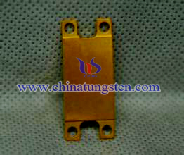
The ways of heat dissipation mainly includes: air heat dissipation, heat the substrate to export, export gold wire cooling, through-hole heat dissipation and so on. Here we introduce the substrate cooling. In LED products typically requires multiple LED assembled on a circuit board. In addition to the circuit board is responsible for carrying LED module structure, on the other hand it also needs to play the role in heat dissipation. LED heat dissipation substrate mainly takes advantages of the excellent heat conductivity of its thermal substrate material to derived from the LED grain. Thus according to the ways of LED heat dissipation, can be divided into two types, LED grain board and the system circuit board. These two are multiplied by different heat dissipation board carrying the LED chip LED grain and the LED grain emits light generated by the circuit board to the system, and then absorbed by the atmosphere via the heat dissipating board LED die, to achieve the dissipation of the heat effect. Tungsten copper material has high strength, low coefficient of thermal expansion, excellent plasticity and thermal and electrical conductivity, which is the perfect choice for LED board. Compared with single metal, such as Al substance, it can avoid the thermal mismatch and have better stability and heat dissipation.
| Tungsten Copper Supplier: Chinatungsten Online tungsten-copper.com | Tel.: 86 592 5129696; Fax: 86 592 5129797;Email:sales@chinatungsten.com |
| Tungsten News & Prices, 3G Version: http://3g.chinatungsten.com | Molybdenum News & Molybdenum Price: http://news.molybdenum.com.cn |
Tungsten Heater for Vacuum Aluminizing - Mirror Industry
- Details
- Category: Tungsten Information
- Published on Tuesday, 28 June 2016 17:32
Mirror is one of the daily commodities. Development of the mirror has experienced three stages: copper, mercury and silver, and with the development of science and technology, vacuum aluminizing has been widely used in mirror industry. Although the history of silver mirror is long and the manufacturing process is more maturity. However, its manufacturing process requires a lot of silver, so it has a great damage for environmental. In addition, the stability of the quality of the product is not enough. Especially in summer, mirror is easy to be damp and silver layer is easy to metamorphose. Therefore, when aluminum mirror was launched, it is popular with the majority of manufacturers. This mirror is made by a new manufacturing process of vacuum aluminizing which evaporate an aluminum film to glass by tungsten heater in vacuum. Two kinds of mirror looks the same, but the mirror of aluminum mirror is blue, the light is soft, silver mirror is white.
Mirror made by vacuum aluminizing has the following excellent features: on the one hand, it is using a vacuum physical vapor deposition, chemical adsorption-based, aluminum film can be well combined with glass, which has a good adhesion. Therefore, the wear resistance of aluminum mirror is strong with long life time. On the other hand, gas molecules of aluminum deposited in vacuum is meticulous, so that the film coated on the glass surface is more uniform with less trachoma, which can improve the corrosion resistance of aluminum mirror, it can be placed in the kitchen and bathroom.
Another point is that vapor deposition of aluminum is from ultraviolet to infrared, because the infrared have relatively high and flat spectral reflectance, reflectance of aluminum mirror in the visible light field can reach more than 90%, which has a higher reflectivity rate and it can reflect image clearly.
However, alkaline resistance of aluminum mirror is poor, which cannot be wiped with a cloth with alkali.

| Tungsten Metals Supplier: Chinatungsten Online www.tungsten.com.cn | Tel.: 86 592 5129696; Fax: 86 592 5129797;Email:sales@chinatungsten.com |
| Tungsten News & Prices, 3G Version: http://3g.chinatungsten.com | Molybdenum News & Molybdenum Price: http://news.molybdenum.com.cn |
Gradient Tungsten Carbide Coated Inserts
- Details
- Category: Tungsten Information
- Published on Tuesday, 28 June 2016 15:23
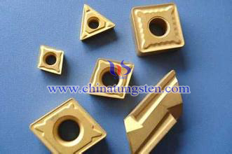
Although tungsten carbide has uniform composition and distribution and compared with other materials has many advantages, there is an inevitable contradiction that the balance between hardness and toughness. It also has been an important factor in limiting conventional carbide materials applications. Preparation and use of new technology, the traditional carbide materials exhibit gradient in the structure, can effectively reconcile the internal contradictions of this group. Gradient tungsten carbide coated inserts achieve better performance by gradient distribution, especially has a great advantage in high-performance carbide cutting tools.
After gradient treatment, alloy formation region lack toughness cubic nitrides and carbonitrides in the surface region, the corresponding binder content is higher than the nominal content of the matrix binder. On this basis, using the CVD method or PVD coating deposited on a cemented carbide substrate to get coated gradient cemented carbide. When the coating is formed the crack extended to the toughness of the gradient region, because of its good ductility and toughness, it can effectively absorb energy during crack propagation, thus effectively preventing the internal crack propagation and to improve the performance of carbide cutting tools.
The experiment shows that with the increasing content of Co, the strength, magnetic saturation has been improved, the hardness, magnetism, density of gradient carbide decreased, and the alloy composition gradient structure more obvious, gradient layer is also thicker; while with the increase of the alloy Ti (CN) content, hardness gradient alloy structure, the magnetic force is increased, reducing the strength and density occurs, reducing the thickness of the alloy graded layer; in the substrate and coating composition of the same situation, coated carbide blade cutting gradient structure without gradient structure coated carbide cutting inserts more excellent (at the same height wear conditions, cutting tool life increased nearly doubled). In addition, higher Co content gradient coated carbide cutting inserts generally better than a low Co content gradient coating blade cutting performance.
| Tungsten Carbide Supplier: Chinatungsten Online tungsten-carbide.com.cn | Tel.: 86 592 5129696; Fax: 86 592 5129797;Email:sales@chinatungsten.com |
| Tungsten News&Tungsten Prices, 3G Version: http://3g.chinatungsten.com | Molybdenum News & Molybdenum Price: http://news.molybdenum.com.cn |
Sputter Targets Prepared by Tungsten Powder
- Details
- Category: Tungsten Information
- Published on Monday, 27 June 2016 18:09
| Tungsten Powder Supplier: Chinatungsten Online tungsten-powder.com | Tel.: 86 592 5129696; Fax: 86 592 5129797;Email:sales@chinatungsten.com |
| Tungsten News & Prices, 3G Version: http://3g.chinatungsten.com | Molybdenum News & Molybdenum Price: http://news.molybdenum.com.cn |
Tungsten Powder and Sputter Targets
- Details
- Category: Tungsten Information
- Published on Monday, 27 June 2016 18:06
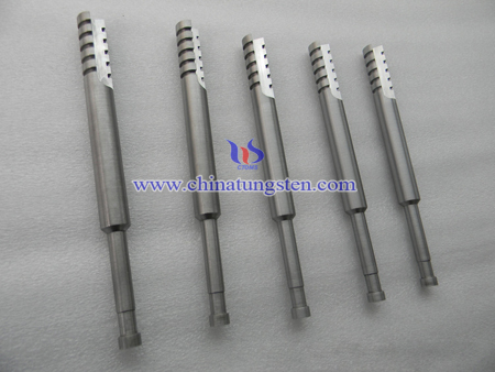
| Tungsten Powder Supplier: Chinatungsten Online tungsten-powder.com | Tel.: 86 592 5129696; Fax: 86 592 5129797;Email:sales@chinatungsten.com |
| Tungsten News & Prices, 3G Version: http://3g.chinatungsten.com | Molybdenum News & Molybdenum Price: http://news.molybdenum.com.cn |
Life Time of Tungsten Heater of Kinescope Evaporation - Heat Treatment
- Details
- Category: Tungsten Information
- Published on Monday, 27 June 2016 14:55
In the process of kinescope evaporation, surface of wire would change and produce crystalline structure because of temperature, it would greatly shorten the life of the heater when the crystal structure increase to a certain number. Therefore, manufacturers should pay attention to control the number of crystal structure of wire surface in the deposition process. In addition, the more the amount of aluminum insertion, the shorter the tungsten heater life time, so the amount of aluminum insertion should not exceed the amount of theory evaporation.
In addition to these two reasons, the fluidity of aluminum has a great impact on the life time of tungsten heater in vapor deposition process. The fluidity of aluminum tungsten is measured by the amount of coil wetted on wolfram twisted spiral surface. The greater the number of spiral turns soaked, the better the fluidity of aluminum. If the Al liquidity is better, aluminum on the surface of the screw would be less after each deposition, the chance of reaction with tungsten would be less, which can prolong life time of tungsten heater. On the contrast, if the liquid of aluminum is poor, then residual aluminum would be deposited on tungsten surface for a long-term after each deposition. Thereby shortening the life time of the heater element.
The heat treatment temperature has a great impact on the life time of heater element. In order to increase its service life, tungsten heater would be placed in the furnace, keep warm for 10 minutes under the conditions of 1400 ℃, and then do heat treatment. When the heat treatment temperature is higher than 1450 ℃, the wire would completely recrystallized, so the spiral would become very brittle, it would break once it is to be touched and cannot be used again. If the heat treatment temperature is lower than 1350 ℃, then it cannot eliminate interior stress generated in the process of wire deformation, which would also reduce its life time. Therefore, control heat treatment temperature is essential for life time of wolfram heater.

| Tungsten Metals Supplier: Chinatungsten Online www.tungsten.com.cn | Tel.: 86 592 5129696; Fax: 86 592 5129797;Email:sales@chinatungsten.com |
| Tungsten News & Prices, 3G Version: http://3g.chinatungsten.com | Molybdenum News & Molybdenum Price: http://news.molybdenum.com.cn |
Tungsten Powder and Electrolytic Capacitor
- Details
- Category: Tungsten Information
- Published on Friday, 24 June 2016 18:11
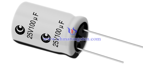
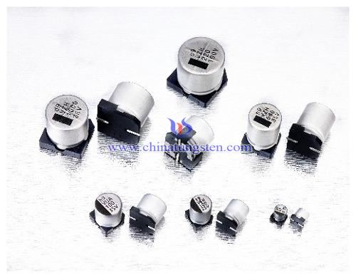
| Tungsten Powder Supplier: Chinatungsten Online tungsten-powder.com | Tel.: 86 592 5129696; Fax: 86 592 5129797;Email:sales@chinatungsten.com |
| Tungsten News & Prices, 3G Version: http://3g.chinatungsten.com | Molybdenum News & Molybdenum Price: http://news.molybdenum.com.cn |
Tungsten Carbide Button — Profile Optimization
- Details
- Category: Tungsten Information
- Published on Friday, 24 June 2016 18:09
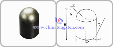
Most of tungsten carbide button profiles are round and bullet-shaped. But in the process of using, conventional round tungsten carbide buttons are prone to be passivated and affects the efficiency of drilling; bullet-shaped tungsten carbide button has tapered crown and small ball radius, so it will be broken easily because of the deficiency in matrix strength in the large impacting power and the hard rock formation. Therefore, tungsten carbide button profile has a significant effect on the performance, which button profile optimization becomes a direction of research.
Based on spherical stamper effective rock breaking mechanism and constant bending stress theory, domestic researchers design blunt-resistant button. It combines the advantages of round buttons and bullet-shaped buttons, the crown consists of spherical shape cap and approximate cone; Wherein the body is subjected to the spherical cap spherical stamper rock breaking, approximate cone dovetail die broken rock, broken rock dominated the first spherical stamper, the stamper wedge after breaking rock, giving the formation of a common rock-breaking effect. In addition, by analyzing the stress distribution of the rock under the spherical die and wedge die proved more rock-breaking effects resistant carbide ball blunt teeth, drilling speed faster, and better impact toughness, not easy to be passivated.
There are experimental data shows that adopt blunt-resistant carbide button, the life and average drilling rate is 36% and 28% higher than bullet-shaped buttons. Another optimized button is composed of fore super-hard sphere and secondary super-hard sphere, the fore super-hard sphere produces shear after breaking rocks; when the drill impacts the rock again, the secondary super-hard sphere impacts on the shear and breaks the rocks repeatedly. This makes carbide button drill bit when drilling footage longer need to drill and drill bit protrusion treatment, but also to maintain a good rock fragmentation capability and self-sharpening performance.
| Tungsten Carbide Supplier: Chinatungsten Online tungsten-carbide.com.cn | Tel.: 86 592 5129696; Fax: 86 592 5129797;Email:sales@chinatungsten.com |
| Tungsten News&Tungsten Prices, 3G Version: http://3g.chinatungsten.com | Molybdenum News & Molybdenum Price: http://news.molybdenum.com.cn |
Tungsten Carbide Button — Ultra-fine Crystallization and Gradient Optimization
- Details
- Category: Tungsten Information
- Published on Friday, 24 June 2016 18:07
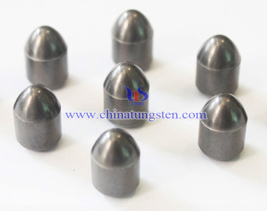
Tungsten carbide button is a kind of rock drilling tools composed of hard phase WC and binder phase Co and has high hardness, high strength, high wear resistance and good impact toughness. Compared similar products with other materials, it has higher drilling speed, extends the service life 5 – 6 times, which not only saves time, improves the efficiency, but also reduces the frequency of changing buttons and manual labor.
With the increasing complexity of environmental conditions, drilling of drill performance requirements are also increasing, especially the button used for high-pressure drilling not only high hardness and wear resistance, but also need good toughness to prevent brittle fracture. The fine grain structure can effectively improve the performance of the alloy, studies have shown that ultrafine-grained and nano-structured carbide button binder phase content in the same case, when the WC grain size of less than 1μm, the hardness and strength can be greatly improved, and with the further reduction in WC grain size, the performance increase rate is more significant. Although nano grain is small in size, it has larger specific surface area, higher surface activity. So it has some excellent properties of nanostructures, such as lowering the sintering temperature required to increase the hardness, strength, wear resistance and impact toughness of mono button, life extension and so on, is one of the hotspots carbide materials currently.
Gradient carbide is a kind of multi-phase structured carbide that developed in the end of 1980s. The most outstanding characteristic is the gradient component and distribution. The preparation principle gradient structure of cemented carbide is obtained using low-carbon carbide alloy containing η phase by vacuum sintering, and treated to alter the distribution of Co binder phase of different parts of button distributed in different carburizing atmosphere Co content. As a result the organizational structure of tungsten carbide button shows gradient distribution of Co, the outer layer – Co-depleted layer, the intermediate layer – Co-rich layer, the inner layer – WC, Co, η three phases microstructure. The outer layer due to the high content of WC has good wear resistance; the intermediate layer has higher content of Co, so the toughness is better.
| Tungsten Carbide Supplier: Chinatungsten Online tungsten-carbide.com.cn | Tel.: 86 592 5129696; Fax: 86 592 5129797;Email:sales@chinatungsten.com |
| Tungsten News&Tungsten Prices, 3G Version: http://3g.chinatungsten.com | Molybdenum News & Molybdenum Price: http://news.molybdenum.com.cn |



 sales@chinatungsten.com