Modelling Plastic Stress Relaxation in Shaped Sapphire Crystal Growth
- Details
- Category: Tungsten & Sapphire Growth Furnace News
- Published on Thursday, 26 December 2013 10:57
Thermally induced stresses in growing shaped sapphire crystals are modelled using transient finite element 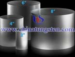 simulations. Boundary conditions and mass changes are fixed on an expanding remeshed and updated grid. The actual stresses are obtained taking into account plastic relaxation through dislocation glide along basal, prismatic and pyramidal slip planes. For this purpose, phenomenological creep laws available for this material are implemented in the frame of thermally activated plasticity. The model is calibrated by comparison with directional mechanical tests, and validation is performed by growth simulations and dislocation density measurements on as-grown crystals.
A two-dimensional, quasi-steady-state, thermal-capillary model is developed for a micro-pulling-down (μ-PD) system to study limitations to steady growth of sapphire. The model incorporates mass, energy, and momentum conservation equations, and also accounts for the physics of the melt meniscus, the solidification front, and the crystal radius. Limit points with respect to pull rate are found under higher-gradient thermal conditions but are shown to unfold with changes in die heating and ambient temperature. Limit points related to crystal size and capillary effects are also found with respect to static head (melt height); however, classical criteria of capillary instability are shown to be invalid. Thus, a more fundamental understanding is obtained for μ-PD operating limits, their origins, and their possible avoidance.
Tungsten Manufacturer & Supplier: Chinatungsten Online - http://www.chinatungsten.com
Tel.: 86 592 5129696; Fax: 86 592 5129797
Email: sales@chinatungsten.com
Tungsten & Molybdenum Information Bank: http://i.chinatungsten.com
Tungsten News & Tungsten Prices, 3G Version: http://3g.chinatungsten.com
Molybdenum News & Molybdenum Price: http://news.molybdenum.com.cn
Orientation Relationships of Zinc Oxide on Sapphire in Heteroepitaxial Chemical Vapor Deposition
- Details
- Category: Tungsten & Sapphire Growth Furnace News
- Published on Wednesday, 25 December 2013 11:42
The anisotropy in ZnO heteroepitaxial growth by CVD is studied on spherical and lens-shaped sapphire  substrates. The layers of ZnO form maps containing many regions of single-crystals of various orientations. By combining equivalent types of these regions, six different modes in the orientation relationships between ZnO and sapphire are distinguished and classified. The effects of growth temperature and reaction gas velocity on the kinds and the extent of these regions are also investigated. The results, drawn by stereographic projection, may provide a useful guide for selecting and preparing substrate planes to obtain specific ZnO planes of high quality, i.e. smooth surface, high perfection, high electron mobility etc.
Chemically vapour deposited silicon on sapphire (SOS) films 0.25 μm thick were implanted with 28Si+ and recrystallized in solid phase by furnace annealing (FA) and IR rapid thermal annealing (RTA) in the laboratory. An improvement in crystalline quality can be obtained using both annealing procedures. After FA, it is hard to retain the intrinsic high resistivity value (104–105 Ω cm) observed in as-grown SOS films, so the improvement process cannot be put to practical use effectively. However, it is demonstrated that by properly adjusting the implantation and RTA conditions, significant improvements in both film quality and film autodoping can be accomplished. This work describes a modified double solid phase epitaxy process in which the intrinsic high resistivities of the as-grown SOS films are retained. The mechanism of suppression of Al autodoping is discussed.
Tungsten Manufacturer & Supplier: Chinatungsten Online - http://www.chinatungsten.com
Tel.: 86 592 5129696; Fax: 86 592 5129797
Email: sales@chinatungsten.com
Tungsten & Molybdenum Information Bank: http://i.chinatungsten.com
Tungsten News & Tungsten Prices, 3G Version: http://3g.chinatungsten.com
Molybdenum News & Molybdenum Price: http://news.molybdenum.com.cn
Ti-Doped Sapphire (Al2O3) Single Crystals Grown by The Kyropoulos Technique And Optical Characterizations
- Details
- Category: Tungsten & Sapphire Growth Furnace News
- Published on Wednesday, 25 December 2013 11:27
Sapphire (α-Al2O3) single crystals grown using the Verneuil and Kyropoulos methods have been analyzed 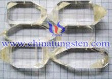 using electron paramagnetic resonance and γ-ray spectroscopy with 12-MeV bremsstrahlung excitation. It is established that uncontrolled impurities in the final sapphire single crystals grown by the Kyropoulos method in molybdenum-tungsten crucibles are supplied both from the initial materials and from the furnace and crucible materials.
Transparent high optical quality and large Ti-sapphire (Ti3+-doped Al2O3) single crystals have been grown by the Kyropoulos technique (KT) for optical amplification. The present work shows that by the utilization of KT growth technology and the optimization of the growth conditions it is possible to grow Ti-doped Al2O3, 100 mm in diameter and 5 kg in weight. We have demonstrated that large Ti(0.25 atom %)-doped Al2O3 crystals show high chemical homogeneities and good optical properties and amplify the energy without any special annealing. Ti-doped sapphire crystals are for high power laser applications and particularly for the shortest pulses ever produced from a laser oscillator.
Tungsten Manufacturer & Supplier: Chinatungsten Online - http://www.chinatungsten.com
Tel.: 86 592 5129696; Fax: 86 592 5129797
Email: sales@chinatungsten.com
Tungsten & Molybdenum Information Bank: http://i.chinatungsten.com
Tungsten News & Tungsten Prices, 3G Version: http://3g.chinatungsten.com
Molybdenum News & Molybdenum Price: http://news.molybdenum.com.cn
Positioning Growth of ZnO Whiskers/Dots on Sapphire Substrates
- Details
- Category: Tungsten & Sapphire Growth Furnace News
- Published on Tuesday, 24 December 2013 15:28
Micro-nano ZnO whiskers and dots have been selectively grown on sapphire substrate using Au/Pt catalyst  arrays. The catalyst array was fabricated by employing a nanoindentation tester, which is simpler than conventional micro-nano fabrication techniques. The electric current heating (ECH) method was used to provide ZnO sources from a ZnO ceramic bar heated to about 1000 °C. The whiskers and dots were grown in the Vapor–Liquid–Solid (VLS) growth mode inside a gold image furnace. SEM images identified dramatic differences in the crystal structures grown at 940 °C, specifically, whiskers for Au catalyst and dots for Pt catalyst.
Whiskers are characterized by diameters of 10 nm to sub-micron and lengths from sub-microns to tens of microns. Dots, however, have a uniform diameter of about 100 nm. We found growth beginning at the arrayed Au catalyst positions. In contrast, dots were formed, but no whiskers were observed around the Pt catalyst. These features are explained in terms of different catalyst melting points: VLS growth was realized for the Au catalyst but not for the Pt catalyst at 940 °C. Good to excellent quality ZnO whisker and dot crystals was confirmed by micro-photoluminescence (PL) measurement.
Tungsten Manufacturer & Supplier: Chinatungsten Online - http://www.chinatungsten.com
Tel.: 86 592 5129696; Fax: 86 592 5129797
Email: sales@chinatungsten.com
Tungsten & Molybdenum Information Bank: http://i.chinatungsten.com
Tungsten News & Tungsten Prices, 3G Version: http://3g.chinatungsten.com
Molybdenum News & Molybdenum Price: http://news.molybdenum.com.cn
Formation of Large-Area Freestanding Gallium Nitride Substrates by Natural Stress-Induced Separation of GaN And Sapphire
- Details
- Category: Tungsten & Sapphire Growth Furnace News
- Published on Tuesday, 24 December 2013 15:18
This paper addresses the formation of freestanding GaN substrates by a natural separation mechanism,  effectively eliminating the need for post-growth processes such as laser liftoff, chemical etching or mechanical lapping to form freestanding GaN substrates. A number of GaN thick films were grown onto sapphire substrates by the hydride vapor-phase epitaxy (HVPE) method with thickness varying from 200 μm to 3.8 mm using either a low-temperature GaN or an AlN buffer as the nucleation step. We have found that samples grown on a low temperature GaN buffer naturally delaminate from the sapphire substrate post-growth over the entire thickness range studied. Furthermore, we have observed that the thinner films have high crack densities leading to the delamination of several smaller freestanding pieces. As the GaN thickness increases, the area of the delaminated pieces also increases, ultimately leading to a 1-to-1 correlation between initial sapphire substrate area and freestanding GaN area. However, the GaN films grown on AlN buffers did not delaminate. These results were accounted for by calculating the thermal stresses in the GaN film and substrate as a function of film thickness using Stoney's equation and assuming that the GaN buffer undergoes decomposition at the growth temperature.
Catalytic growth of GaN nanowires by hydride vapour phase epitaxy is demonstrated. Nickel–gold was used as a catalyst. Nanowire growth was limited to areas patterned with catalyst. Characterization of the nanowires with transmission electron microscopy, x-ray diffraction, and low temperature photoluminescence shows that the nanowires are stoichiometric 2H-GaN single crystals growing in the orientation when grown on sapphire, with occasional stacking faults along the c-axis as the only defect type observed in most of the wires. A red shift observed in the photoluminescence was too large to be explained by the minor strain observed alone, and was only marginally affected by temperature, suggesting a superposition of several factors.
Tungsten Manufacturer & Supplier: Chinatungsten Online - http://www.chinatungsten.com
Tel.: 86 592 5129696; Fax: 86 592 5129797
Email: sales@chinatungsten.com
Tungsten & Molybdenum Information Bank: http://i.chinatungsten.com
Tungsten News & Tungsten Prices, 3G Version: http://3g.chinatungsten.com
Molybdenum News & Molybdenum Price: http://news.molybdenum.com.cn
80-mm EFG Sapphire Dome Blanks Yield High-Quality Low-Cost Single-Crystal Domes
- Details
- Category: Tungsten & Sapphire Growth Furnace News
- Published on Monday, 23 December 2013 11:53
Close attention to crystal growth parameters and characterization of the crystal's thermal environment during  growth has led to improvement in the crystal structure of EFG grown dome blanks. These near net shape 80 mm sapphire blanks have been fabricated to produce high quality finished domes. New measurements of the coefficient of thermal expansion (CTE), thermal conductivity, optical scatter, rain erosion and the thermal coefficient of refractive index (dn/dT) as a function of wavelength have been performed and the data are presented.
It presents dynamic 3D finite element simulation of stress and deformation of growing thin-walled, polygonal tubes. As an example, the growth of octagonal silicon tubes by the edge-defined film-fed growth (EFG) method is chosen. In tubes with wall thickness in the order of several 100 μm the increasing strain energy during growth is periodically reduced by deflections of the walls at regular intervals. The influence of various temperature profiles on the deflection behavior is studied. The applicability of this model to the EFG growth of silicon octagons is discussed by means of experimental observations.
Tungsten Manufacturer & Supplier: Chinatungsten Online - http://www.chinatungsten.com
Tel.: 86 592 5129696; Fax: 86 592 5129797
Email: sales@chinatungsten.com
Tungsten & Molybdenum Information Bank: http://i.chinatungsten.com
Tungsten News & Tungsten Prices, 3G Version: http://3g.chinatungsten.com
Molybdenum News & Molybdenum Price: http://news.molybdenum.com.cn
Substrate Pre-Treatment And Initial Growth:Strategies Towards High-Quality III-Nitride Growth on Sapphire by Molecular Beam Epitaxy
- Details
- Category: Tungsten & Sapphire Growth Furnace News
- Published on Monday, 23 December 2013 11:23
Sapphire substrates annealed at 1200 °C in N2 : O2 (3 : 1) developed terrace-and-step morphology, ideal for 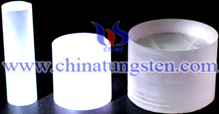 III-nitride growth by molecular beam epitaxy. In situ treatment of sapphire substrates, using Ga deposition and desorption prior to growth, is shown to be negative for GaN growth. Nitridation transforms the sapphire substrate surface to a lateral structure similar to AlN (mismatch < 2.5%). The surface lattice parameters after nitridation did not depend on the substrate temperature. AlN nucleation layer growth conditions have been optimized for growth of GaN. Ideal Al / N flux ratio was found to be 0.6 for a 9 nm thick nucleation layer.
ZnO nanowires were fabricated on Au coated sapphire substrates by using a pulsed Nd:YAG laser with a ZnO target in furnace. ZnO nanowires have various sizes and shapes with a different substrate position inside a furnace. The length and the diameter of these ZnO nanowires were around 3–4 μm and 120–200 nm, respectively, confirmed by scanning electron microscopy (SEM). The diameter control of the nanowires was achieved by varying the position of substrates. The ultraviolet emission of nanowires from the near band-edge emission (NBE) was observed at room temperature. The formation mechanism and the effect of different position of substrates on the structural and optical properties of ZnO nanowires are discussed.
Tungsten Manufacturer & Supplier: Chinatungsten Online - http://www.chinatungsten.com
Tel.: 86 592 5129696; Fax: 86 592 5129797
Email: sales@chinatungsten.com
Tungsten & Molybdenum Information Bank: http://i.chinatungsten.com
Tungsten News & Tungsten Prices, 3G Version: http://3g.chinatungsten.com
Molybdenum News & Molybdenum Price: http://news.molybdenum.com.cn
A Second Specific Embodiment of The Three Groups Nitride Based Compound Semiconductor Laser Diode
- Details
- Category: Tungsten & Sapphire Growth Furnace News
- Published on Friday, 20 December 2013 10:17
The sapphire substrate with the Group III nitride compound semiconductor laser element layer thus formed  was dipped in a HCl base etchant that was held at 60°C. The substrate was then loaded in an ultrasonic cleaner for about 10 min so as to perform selective etching of the intermediate ZnO layer. As a result, the intermediate ZnO layer was removed to form a grid pattern of gaps between the sapphire substrate and the Si-doped, n-type GaAlN layer(n layer) which was the bottommost part of the semiconductor laser element layer.
In the next step, a sharp blade positioned right above each of the gaps was compressed onto the top surface of the SiO2 layer along line C-C, whereby the semiconductor laser element layer composed of three sublayers was cleaved. The resulting end faces of the cleavage would eventually serve as the mirror surfaces of a laser cavity.
Tungsten Manufacturer & Supplier: Chinatungsten Online - http://www.chinatungsten.com
Tel.: 86 592 5129696; Fax: 86 592 5129797
Email: sales@chinatungsten.com
Tungsten & Molybdenum Information Bank: http://i.chinatungsten.com
Tungsten News & Tungsten Prices, 3G Version: http://3g.chinatungsten.com
Molybdenum News & Molybdenum Price: http://news.molybdenum.com.cn
Three Specific Embodiments Nitride Based Compound Semiconductor Laser Diode
- Details
- Category: Tungsten & Sapphire Growth Furnace News
- Published on Friday, 20 December 2013 10:02
The steps of forming a semiconductor laser element layer on the thus processed sapphire substrate will now 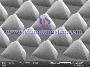 be described with reference is a section A-A is a section B-B. In other words, the direction is cut to produce section A-A is perpendicular to the direction is cut to produce section B-B.
The substrate was cooled to a temperature of about 600°C and trimethyl aluminum (TMA) and ammonia (NH3) were supplied to form an AlN layer 18 with a uniform thickness of about 50 nm on the substrate.Subsequently, only the supply of TMA was stopped and the substrate temperature was raised to 1040°C, followed by the supply of TMA, trimethyl gallium (TMG) and silane (SiH4) to have a Si-doped, n-type GaAlN layer 13 (n layer) formed on the AlN layer.
Tungsten Manufacturer & Supplier: Chinatungsten Online - http://www.chinatungsten.com
Tel.: 86 592 5129696; Fax: 86 592 5129797
Email: sales@chinatungsten.com
Tungsten & Molybdenum Information Bank: http://i.chinatungsten.com
Tungsten News & Tungsten Prices, 3G Version: http://3g.chinatungsten.com
Molybdenum News & Molybdenum Price: http://news.molybdenum.com.cn
Three Nitride Based Compound Semiconductor Laser Diode Object of The Invention
- Details
- Category: Tungsten & Sapphire Growth Furnace News
- Published on Thursday, 19 December 2013 10:22
Objective three nitride based compound semiconductor laser diode of the present invention is to provide a III  nitride semiconductor on a sapphire substrate, formed thereon and provided with a sufficiently high quality splitting surface to generate a higher laser the output of the laser element layer.
The above object of the three groups nitride based compound semiconductor laser diode of the invention can be manufactured by a laser diode group III nitride compound semiconductor to achieve (; 0 ≤ X ≤ 1; (the Al x Ga-X) yIn1-YN 0 ≤ Y ≤ 1) as defined in claim 1 having a double hetero junction structure is maintained between the layer having a larger band gap of the active layer.
Tungsten Manufacturer & Supplier: Chinatungsten Online - http://www.chinatungsten.com
Tel.: 86 592 5129696; Fax: 86 592 5129797
Email: sales@chinatungsten.com
Tungsten & Molybdenum Information Bank: http://i.chinatungsten.com
Tungsten News & Tungsten Prices, 3G Version: http://3g.chinatungsten.com
Molybdenum News & Molybdenum Price: http://news.molybdenum.com.cn


 sales@chinatungsten.com