Three Specific Embodiments Nitride Based Compound Semiconductor Laser Diode
- Details
- Category: Tungsten & Sapphire Growth Furnace News
- Published on Friday, 20 December 2013 10:02
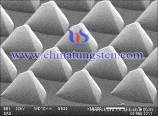
The steps of forming a semiconductor laser element layer on the thus processed sapphire substrate will now  be described with reference is a section A-A is a section B-B. In other words, the direction is cut to produce section A-A is perpendicular to the direction is cut to produce section B-B.
The substrate was cooled to a temperature of about 600°C and trimethyl aluminum (TMA) and ammonia (NH3) were supplied to form an AlN layer 18 with a uniform thickness of about 50 nm on the substrate.Subsequently, only the supply of TMA was stopped and the substrate temperature was raised to 1040°C, followed by the supply of TMA, trimethyl gallium (TMG) and silane (SiH4) to have a Si-doped, n-type GaAlN layer 13 (n layer) formed on the AlN layer.
Tungsten Manufacturer & Supplier: Chinatungsten Online - http://www.chinatungsten.com
Tel.: 86 592 5129696; Fax: 86 592 5129797
Email: sales@chinatungsten.com
Tungsten & Molybdenum Information Bank: http://i.chinatungsten.com
Tungsten News & Tungsten Prices, 3G Version: http://3g.chinatungsten.com
Molybdenum News & Molybdenum Price: http://news.molybdenum.com.cn


 sales@chinatungsten.com