High Performance Thin-Film Flip-Chip InGaN–GaN Light-Emitting Diodes
- Details
- Category: Tungsten & Sapphire Growth Furnace News
- Published on Saturday, 08 February 2014 11:48
Data are presented on the operation of thin-film flip-chip InGaN/GaN multiple-quantum-well light-emitting  diodes (LEDs). The combination of thin-film LED concept with flip-chip technology is shown to provide surface brightness and flux output advantages over conventional flip-chip and vertical-injection thin-film LEDs. Performance characteristics of blue, white, and green thin-film flip-chip 1×1 mm2 LEDs are described. Blue (∼441 nm) thin-film flip-chip LEDs are demonstrated with radiance of 191 mW/mm2 sr at 1 A drive, more than two times brighter than conventional flip-chip LEDs. An encapsulated thin-film flip-chip blue LED lamp is shown to have external quantum efficiency of 38% at forward current of 350 mA. A white lamp based on a YAG:Ce phosphor coated device exhibits luminous efficacy of 60 lm/W at 350 mA with peak efficiency of 96 lm/W at 20 mA and luminance of 38 Mcd/m2 at 1 A drive current. Green (∼517 nm) devices exhibit luminance of 37 Mcd/m2 at 1 A.
We have measured polarized Raman spectra in a 2.0 mu m GaN epitaxial layer of high quality, grown on a sapphire substrate. All symmetry-allowed optical phonons in GaN have been assigned as follows: A1(LO), 735 cm-1; A1(TO), 533 cm-1; E1(LO), 743 cm-1; E1(TO), 561 cm-1; E2, 144 and 569 cm-1. Using the Lyddane-Sachs-Teller relation, the static dielectric constants of GaN for the ordinary and extraordinary directions have been estimated as epsilon perpendicular to 0=9.28 and E/sub //0/=10.1. We have also observed quasi-LO phonons in GaN. A brief discussion on these will be given.
Tungsten Manufacturer & Supplier: Chinatungsten Online - http://www.chinatungsten.com
Tel.: 86 592 5129696; Fax: 86 592 5129797
Email: sales@chinatungsten.com
Tungsten & Molybdenum Information Bank: http://i.chinatungsten.com
Tungsten News & Tungsten Prices, 3G Version: http://3g.chinatungsten.com
Molybdenum News & Molybdenum Price: http://news.molybdenum.com.cn
Self-Separation of A Thick AlN Layer From A Sapphire Substrate Via Interfacial Voids Formed by The Decomposition of Sapphire
- Details
- Category: Tungsten & Sapphire Growth Furnace News
- Published on Wednesday, 29 January 2014 16:14
A technique for separating a thick AlN layer grown by hydride vapor phase epitaxy (HVPE) on a sapphire 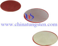 substrate was developed. By heat treatment at 1450 ℃ in a gas flow containing H2 and NH3, many voids could be formed at the interface between a thin (100 nm) AlN layer grown at 1065 ℃ and the sapphire substrate due to the preferential decomposition of sapphire. During the cooling process after the subsequent growth of a thick (85 μm) AlN layer, the thick AlN layer separated from the sapphire substrate with the aid of the interfacial voids. The freestanding AlN substrate thus obtained had a smooth surface, a dislocation density of 1.1× 109 cm-2, and an optical transparency for wavelengths above 208.1 nm.
Single‐crystal layers of AlN have been grown on sapphire substrates between 1000 and 1100 °C by vapor‐phase reaction of aluminum chlorides with ammonia. The purity, color, crystallinity, growth morphology, and electrical resistivity of the epitaxial layers have been investigated. Infrared specular reflection measurements showed the presence of an appreciable strain at the AlN‐sapphire epitaxy interface. Optical absorption data strongly suggest the AlN is a direct band‐gap material with a value of about 6.2 eV at room temperature.
Tungsten Manufacturer & Supplier: Chinatungsten Online - http://www.chinatungsten.com
Tel.: 86 592 5129696; Fax: 86 592 5129797
Email: sales@chinatungsten.com
Tungsten & Molybdenum Information Bank: http://i.chinatungsten.com
Tungsten News & Tungsten Prices, 3G Version: http://3g.chinatungsten.com
Molybdenum News & Molybdenum Price: http://news.molybdenum.com.cn
Enhancing The Output Power of GaN-Based LEDs Grown on Wet-Etched Patterned Sapphire Substrates
- Details
- Category: Tungsten & Sapphire Growth Furnace News
- Published on Wednesday, 29 January 2014 16:03
GaN-based light-emitting diodes (LEDs) with emitting wavelength of 450 nm were grown on patterned sapphire 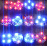 substrates (PSSs) fabricated by chemical wet etching. The crystallography-etched facet was R-plane with a 57deg against C-axis and had superior capability for enhancing light extraction efficiency. The light output power of the PSS LED was 1.15 times higher than that of the conventional LED at an injection current of 20 mA. The output power and external quantum efficiency were estimated to be 9 mW and 16.4%, respectively. The improvement was attributed not only to geometrical shapes of {1-102} crystallography-etched facets that efficiently scatter the guided light to find escape cones, but also to dislocation density reduction by adopting the PSS growth scheme.
Lattice constants of gallium nitride (wurzite structure) have been measured at temperatures 294–753 K. The measurements were performed by using x‐ray diffractometry. Two kinds of samples were used: (1) bulk monocrystal grown at pressure of 15 kbar, (2) epitaxial layer grown on a sapphire substrate. The latter had a smaller lattice constant in a direction parallel to the interface plane by about 0.03%. This difference was induced by a higher thermal expansion of the sapphire with respect to the GaN layer. However, this thermal strain was created mainly at temperatures below 500–600 K. Above these temperatures the lattice mismatch in parallel direction diminished to zero at a temperature of about 800 K.
Tungsten Manufacturer & Supplier: Chinatungsten Online - http://www.chinatungsten.com
Tel.: 86 592 5129696; Fax: 86 592 5129797
Email: sales@chinatungsten.com
Tungsten & Molybdenum Information Bank: http://i.chinatungsten.com
Tungsten News & Tungsten Prices, 3G Version: http://3g.chinatungsten.com
Molybdenum News & Molybdenum Price: http://news.molybdenum.com.cn
Carrier Concentration and Mobility in GaN Epilayers on Sapphire Substrate Studied by Infrared Reflection Spectroscopy
- Details
- Category: Tungsten & Sapphire Growth Furnace News
- Published on Tuesday, 28 January 2014 11:55
We report the measurement of carrier concentration and mobility of metalorganic chemical vapor deposited 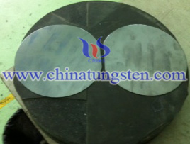 GaN thin films on the sapphire substrate by an infrared reflection technique. By fitting with the experimental data we obtain all the parameters of the lattice vibration oscillators and of the plasmon. From the plasmon frequency and the damping constant we have derived the carrier concentration and the electron mobility. The concentration agrees with the Hall data very well while the mobility values are smaller than that of the Hall measurement by a factor of about 0.5. We attribute such mobility lowering to the increase of scattering for the electrons coupling with the incident photons.
GaN layers are grown on sapphire substrate by electron cyclotron resonance molecular beam epitaxy (ECR-MBE) using an ECR plasma cell with ion removal magnets on the cell top for the nitrogen source. The efficiency of the ion removal magnets in this ECR plasma cell is 99%. High-quality GaN layers are obtained. In particular, (2×2) and (4×4) RHEED (reflection high-energy electron diffraction) patterns are observed during GaN growth and during cooling after growth, respectively, indicating a flat and smooth surface of GaN. These results show the superiority of the ion-removed ECR plasma cell.
Tungsten Manufacturer & Supplier: Chinatungsten Online - http://www.chinatungsten.com
Tel.: 86 592 5129696; Fax: 86 592 5129797
Email: sales@chinatungsten.com
Tungsten & Molybdenum Information Bank: http://i.chinatungsten.com
Tungsten News & Tungsten Prices, 3G Version: http://3g.chinatungsten.com
Molybdenum News & Molybdenum Price: http://news.molybdenum.com.cn
In Situ Ttemperature Measurements Via Ruby R Lines of Sapphire Substrate Based InGaN Light Emitting Diodes During Operation
- Details
- Category: Tungsten & Sapphire Growth Furnace News
- Published on Tuesday, 28 January 2014 11:40
The temperature of encapsulated green and ultraviolet light emitting diodes (LEDs) in operation has been 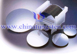 measured optically via the ruby R lines emitted by the residual Cr3+ contaminations in the sapphire substrate. These two photoluminescent R lines, which are excited by the electroluminescence of the LED itself, show a well-characterized line shift as a function of temperature and pressure. The temperature is found to rise linearly with the applied forward current of the LED at a rate of ≈1 K/mA. This optical temperature measurement based on monitoring the two ruby R lines could qualify as a sensitive method for an in situ temperature sensor for other sapphire substrate based semiconductor devices such as laser diodes and field effect transistors.
Indium–gallium nitride (InxGa1-xN) single-quantum-well (SQW) light emitting diodes (LEDs), grown by metalorganic chemical vapor deposition on sapphire, were transferred onto Si substrates. The thin-film InxGa1-xN SQW LED structures were first bonded onto a n+-Si substrate using a transient-liquid-phase Pd–In wafer-bonding process followed by a laser lift-off technique to remove the sapphire growth substrate. Individual, 250×250 μm2, LEDs with a backside contact through the n+-Si substrate were then fabricated. The LEDs had a typical turn-on voltage of 2.5 V and a forward current of 100 mA at 5.4 V. The room-temperature emission peak for the InxGa1-xN SQW LEDs was centered at 455 nm with a full width at half maximum of 19 nm.
Tungsten Manufacturer & Supplier: Chinatungsten Online - http://www.chinatungsten.com
Tel.: 86 592 5129696; Fax: 86 592 5129797
Email: sales@chinatungsten.com
Tungsten & Molybdenum Information Bank: http://i.chinatungsten.com
Tungsten News & Tungsten Prices, 3G Version: http://3g.chinatungsten.com
Molybdenum News & Molybdenum Price: http://news.molybdenum.com.cn
High Quality Epitaxial Aluminum Nitride Layers on Sapphire by Pulsed Laser Deposition
- Details
- Category: Tungsten & Sapphire Growth Furnace News
- Published on Monday, 27 January 2014 13:52
We have grown high quality epitaxial AlN layers on sapphire substrates by pulsed laser ablation of a  stoichiometric AlN target. The AlN films deposited at 800 °C and laser energy densities in the range of 2–3 J/cm2 were found to be epitaxial with the c axis normal to the Al2O3 surface. The x‐ray rocking curve of epitaxial AlN films yielded a full width at half maximum of 0.21°. The selected area electron diffraction patterns and high resolution transmission electron microscopy also revealed that the films were epitaxial with an orientational relationship of AlN‖Al2O3 and in‐plain alignment of AlN‖Al2O3 and AlN‖Al2O3. This is equivalent to 30° rotation in the basal plane of the AlN film with respect to the sapphire substrate.
The absorption edge measured by ultraviolet‐visible spectroscopy for the epitaxial AlN film was sharp and the band gap was found to be 6.1 eV. The electrical resistivity of the films was about 5–6×10¹³ ohm cm with a breakdown field of 5×10⁶ V/cm. At higher laser energy densities ≥10 J/cm2 and lower temperatures ≤650 °C, the deposited films were nitrogen deficient and contained free metallic aluminum, both of which degrade the microstructural, electrical, and optical properties of the AlN films.
Tungsten Manufacturer & Supplier: Chinatungsten Online - http://www.chinatungsten.com
Tel.: 86 592 5129696; Fax: 86 592 5129797
Email: sales@chinatungsten.com
Tungsten & Molybdenum Information Bank: http://i.chinatungsten.com
Tungsten News & Tungsten Prices, 3G Version: http://3g.chinatungsten.com
Molybdenum News & Molybdenum Price: http://news.molybdenum.com.cn
Ultraviolet Electroluminescence from N-ZnO:Ga/p-ZnO:N Homojunction Device on Sapphire Substrate with P-Type ZnO:N Layer Formed by Annealing in N2O Plasma Ambient
- Details
- Category: Tungsten & Sapphire Growth Furnace News
- Published on Monday, 27 January 2014 13:34
ZnO homojunction light emitting device (LED) with n-ZnO:Ga/p-ZnO:N structure was fabricated on sapphire  substrate by metal organic chemical vapor deposition. The reproducible p-type ZnO:N layer with hole concentration of 1.29 × 1017 cm−3 was formed with NH3 as N doping source followed by thermal annealing in N2O plasma protective ambient. The device exhibited desirable rectifying behavior. Distinct electroluminescence emission centered at 3.2 eV and 2.4 eV were detected from this device under forward bias at room temperature. The intensive ultraviolet emission was comparable to the visible emission in the electroluminescence spectrum, which represent remarkable progress in the performance of ZnO homojunction LED.
Epitaxial layers of ZnO have been deposited by chemical vapor transport on single‐crystal sapphire substrates. The ZnO layers have been deposited up to thicknesses of 100μ. X‐ray analysis showed that the c axis of the ZnO could be made to lie parallel to the‐oriented sapphire substrate. Resistivities were generally from 1 to 10 Ω‐cm but could be significantly increased by diffusion of lithium or sodium.
Tungsten Manufacturer & Supplier: Chinatungsten Online - http://www.chinatungsten.com
Tel.: 86 592 5129696; Fax: 86 592 5129797
Email: sales@chinatungsten.com
Tungsten & Molybdenum Information Bank: http://i.chinatungsten.com
Tungsten News & Tungsten Prices, 3G Version: http://3g.chinatungsten.com
Molybdenum News & Molybdenum Price: http://news.molybdenum.com.cn
Direct Growth of A-Plane GaN on R-Plane Sapphire Substrate by Metalorganic Vapor Phase Epitaxy
- Details
- Category: Tungsten & Sapphire Growth Furnace News
- Published on Sunday, 26 January 2014 11:53
We have investigated a direct growth of non-polar a-plane GaN on r-plane sapphire substrate by metalorganic  vapor-phase epitaxy (MOVPE). We found that high-density nucleation of GaN islands was grown on r-plane sapphire substrate at an initial stage of high temperature growth without a buffer layer, which resulted in a flat surface of the a-plane GaN. We also studied an effect of growth conditions on surface morphologies and the growth features of the a-plane GaN. The results showed that inverse-triangular pits surrounded with facets were formed at a relatively high V/III ratio, and the lateral growth rate along the c-axis direction was enhanced at a relatively low V/III ratio.
In the present paper we propose to extend the selective epitaxy of GaN to the lateral overgrowth and to take advantage of the growth anisotropy to produce strain free GaN crystals. After filling the openings in a dielectric mask by selective epitaxy, lateral overgrowth occurs reflecting the growth anisotropy. This allows the fabrication of samples with non-planar geometry. The selective epitaxy was achieved by metal organics vapour phase epitaxy (MOVPE) whereas lateral overgrowth until island coalescence was carried out either by MOVPE or halide vapour phase epitaxy (HVPE). A GaN epitaxial layer is first grown using atmospheric pressure metalorganic vapour phase epitaxy on sapphire. The dielectric film is silicon nitride. The openings are achieved using standard photolithographic technology. These openings reveal free GaN surface and are used for epitaxial regrowth by MOVPE, and then by HVPE.
Tungsten Manufacturer & Supplier: Chinatungsten Online - http://www.chinatungsten.com
Tel.: 86 592 5129696; Fax: 86 592 5129797
Email: sales@chinatungsten.com
Tungsten & Molybdenum Information Bank: http://i.chinatungsten.com
Tungsten News & Tungsten Prices, 3G Version: http://3g.chinatungsten.com
Molybdenum News & Molybdenum Price: http://news.molybdenum.com.cn
The Role of Inner And Internal Radiation on The Melt Growth of Sapphire Crystal
- Details
- Category: Tungsten & Sapphire Growth Furnace News
- Published on Sunday, 26 January 2014 11:41
In this paper, for an inductively heated Czochralski furnace used to grow sapphire single crystal, influence of the  inner (wall-to-wall) and crystal internal (bulk) radiation on the characteristics of the growth process such as temperature and flow fields, structure of heat transfer and crystal-melt interface has been studied numerically using the 2D quasi-steady state finite element method. The obtained results of global analysis demonstrate a strong dependence of thermal field, heat transport structure and crystal-melt interface on both types of radiative heat transfer within the growth furnace.
The well-defined and repeatable electrical properties of single-crystal sapphire make it an attractive substrate material for microstrip, but its dielectric anisotropy constitutes an important design complication. This paper describes investigations into the quasi-static characteristics of single microstrip lines on sapphire substrates cut with a specified orientation. To account for anisotropy, a new permittivity parameter epsilonreq is introduced, which is a function of the Iinewidth to substrate-height ratio W/h. The variation of epsilonreq with W/h is derived by finite-difference methods. Universal curves for microstrip on correctly orientated sapphire are presented, showing 1) Epsilonreq, 2)The low-frequency limit of effective microstrip permittivity epsilone0, and 3)The characteristic impedance of the line Z0, all as functions of W/h.
Tungsten Manufacturer & Supplier: Chinatungsten Online - http://www.chinatungsten.com
Tel.: 86 592 5129696; Fax: 86 592 5129797
Email: sales@chinatungsten.com
Tungsten & Molybdenum Information Bank: http://i.chinatungsten.com
Tungsten News & Tungsten Prices, 3G Version: http://3g.chinatungsten.com
Molybdenum News & Molybdenum Price: http://news.molybdenum.com.cn
Power and linearity characteristics of GaN MISFETs on sapphire substrate
- Details
- Category: Tungsten & Sapphire Growth Furnace News
- Published on Friday, 24 January 2014 11:35
The improvement of device performance arising from the adoption of a MIS gate structure in GaN field-effect  transistor (FET) is presented. GaN MISFET/MESFET devices were fabricated on sapphire substrate with and without the insertion of a thin SiN layer on device surface. The MISFET device showed improved device characteristic due to significant reduction in device gate leakage with respect to the standard MESFET structure. Measured power and linearity performance showed promising results. Under single-tone testing at 4 GHz, device yielded saturated output power 6.2 W/mm with 55% peak power added efficiency. When tested with two-tone signal device maintained a carrier to third order intermodulation ratio of 30 dBc up to power levels of 1.8 W/mm with 40% power added efficiency.
GaN films were grown on c‐plane sapphire substrates by low pressure metalorganic chemical vapor deposition using a GaN buffer layer grown at lower temperatures. The quality and surface morphology of the GaN films were strongly affected by the surface pretreatment of the sapphire substrate before the growth of the GaN buffer layer and the GaN epitaxial layer. The films grown on pre‐nitrided sapphire substrates exhibit improved electrical and optical properties over those of the films grown on unnitrided substrates even though the surface morphology became rougher. We have achieved a carrier concentration in the range of 2×10¹⁶–5×1017 cm-3 and electron mobility in the range of 250–300 cm2/V s at room temperature. The GaN films were evaluated by photoluminescence, Hall measurement, x‐ray rocking curve, and transmission electron and scanning electron microscopies.
Tungsten Manufacturer & Supplier: Chinatungsten Online - http://www.chinatungsten.com
Tel.: 86 592 5129696; Fax: 86 592 5129797
Email: sales@chinatungsten.com
Tungsten & Molybdenum Information Bank: http://i.chinatungsten.com
Tungsten News & Tungsten Prices, 3G Version: http://3g.chinatungsten.com
Molybdenum News & Molybdenum Price: http://news.molybdenum.com.cn


 sales@chinatungsten.com