Market Research of Tungsten Wire for Diamond Wire Saws in China's Photovoltaic Industry (I)
- Details
- Category: Tungsten's News
- Published on Thursday, 07 July 2022 20:13
Chapter 1 Basic Concept of Solar Energy, Photovoltaic (PV) & Tungsten Wire
The 2021 edition of "China Potovoltaic Industry Development Roadmap", edited by experts at the China Photovoltaic Industry Association (CPIA) and CCID Thinktank Institute of Integrated Circuits, was released on February 23, 2022, under the guidance of the Ministry of Industry and Information Technology of the People’s Republic of China. Basic on authoritative statistics and basic thinking of the article, China Tungsten Online provides an overview of the background of the development of tungsten wire for main body of diamond wire in China, i.e., the extremely rapid development of China's photovoltaic (PV) industry in recent years and its worldwide position.
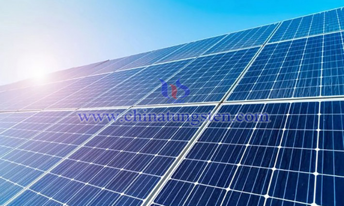
The photovoltaic industry chain includes six major segments. The upstream incorporates phase of silicon material, silicon wafer, including silicon material, silicon ingot, monocrystalline silicon stick and slicing; midstream covers the phase of cell, cell components, including cell, cell components; downstream application systems contain centralized and distributed photovoltaic power station, etc. The industry chain in the PV market shows a pyramid-shaped structure, that is, from a global perspective, the number of companies involved in the six segments increased sharply in sequence.
China's PV manufacturing industry holds first place in the world, with grid-connected PV power generation capacity reaching 306 million kilowatts in 2021, ranking first in the world for seven consecutive years. China's related new energy industry chain is fully benefited amid the context of carbon reduction and carbon neutrality target, overlaid with the gradually eased PV upstream supply chain and demand tension, PV industry continued upward.
According to incomplete statistics, in the first half of 2022, China's new PV installation scale exceeded expectations and the end demand is robust. Since 2022, the policy for supporting PV industry introduced continuously, PV is a significant part of the new energy infrastructure, large base centralized power plants and distributed photovoltaic projects together to promote the industry. In a promising future, new installed capacity is expected to continue to improve, the industry chain boom will be maintained for quite a long time. With the mounting price of energy costs amid the conflict between Russia and Ukraine, upstream silicon material prices will remain high due to the tremendous market demand, which in turn provides investment incentives and profit margins to improve technology, save silicon materials and improve efficiency.
This chapter gives a brief explanation of the three major industries and four materials involved in this research. In principle, the research covers photovoltaic batteries/solar batteries, silicon materials, diamond wire (diamond wire saw, carbon steel wire saw), and tungsten wire. And the involves three industries namely are the silicon wafer cutting industry in PV industry, diamond wire manufacturing, and the tungsten wire processing in the tungsten industry.
1. Solar Batteries
The PV industry is a novel type of industry derived from the combination of semiconductor technology and new energy. Among the various renewable energy sources, solar energy with its significant advantages of clean, safe, and inexhaustible, becoming the fastest growing renewable energy. Vigorous development of PV industry, is of great significance to adjust the energy structure, promote energy production and consumption revolution, as well as boost the construction of ecological civilization. China has listed PV industry as one of the national strategic emerging industries, and under the dual role of industrial policy guidance and market demand, China's PV industry has achieved rapid development and has become one of the few domestic industries that could participate in international competition and achieve a leading edge. West major developed countries are also taking the development and utilization of solar energy as a long-term plan for the energy revolution, and the PV industry is increasingly becoming another exploding development industry in the international arena following the IT and microelectronics industries.
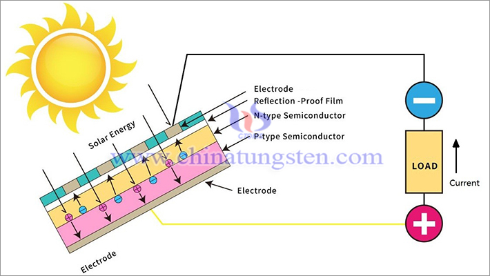
Photovoltaic effect (PV Effect) is a process by which light excitation causes a semiconductor material to generate electron-hole pairs and form an electrical potential for P-N junction and separation. Solar battery uses the PV effect of the semiconductor materials to convert solar energy into electricity. Solar battery is mainly connected in series connection and parallel connection to produce the required voltage and current. The battery is divided into two types: space-based solar power and ground-mounted solar panels. The main requirements for space-based are light weight, high conversion efficiency, and radiation resistance, etc.; and the ground-mounted one requires high conversion efficiency and low cost. Solar power products have been widely applied in communications, lighting, traffic signals, beacon lights, home appliances, cathode protection, remote control instruments, water pumps, consumer goods (such as calculators, electronic watches), etc. Monocrystalline silicon solar batteries and gallium arsenide solar batteries are also used as power sources for artificial satellites.
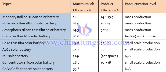
Materials used for solar batteries include monocrystalline silicon, polycrystalline silicon (see semiconductor silicon materials), gallium arsenide monocrystal, indium phosphide monocrystal, gallium antimonide monocrystal, and amorphous silicon film (see amorphous semiconductor materials), copper indium tin (see compound semiconductor materials), cadmium telluride film, and cadmium sulfide film.
2. Silicon Photovoltaic Materials
Silicon (Si) is the most important elemental semiconductor material, including polycrystalline silicon, monocrystalline silicon, silicon wafer, silicon epitaxy wafer, and amorphous silicon film, etc., which can be used directly or indirectly to prepare semiconductor devices. Si is a group IV element in the periodic table and exists in the earth's crust mainly in the form of silica and silicates. Si has an atomic weight of 28.05 and a density of 2.329 g/cm3 at 25°C. It has a gray metallic luster, is brittle, with a hardness of 6.5 Mohs, which is slightly lower than that of quartz, the melting point is 1410°C with a volume shrinkage of 9.5% at the melting point. Si is available in crystalline and amorphous forms. Monocrystalline silicon hosts a dielectric coefficient of 11.7 at room temperature and a high refractive index of light (n=3.42), with a large reflection loss, which can be greatly improved by applying reflective film.
Si exists in three forms: amorphous, polycrystalline and monocrystalline. Compared to monocrystalline silicon, polycrystalline silicon has no fixed crystal orientation, its structural integrity is poor, and most devices are made from monocrystalline silicon. Monocrystalline silicon stick made by methods such as hydrogen reduction or thermal decomposition of silane are mainly used for producing monocrystalline silicon.
![]()
2.1 Crystalline Silicon Materials
2.2 Polycrystalline Silicon
2.3 Monocrystalline Silicon
3. Wire Saw
3.1 Free Abrasive Wire Saw
3.2 Coated Abrasive Wire Saw
3.3 Resin-Bonded Coated Abrasive Wire Saw
3.4 Electroplated Coated Abrasive Wire Saw
3.5 Diamond Wire Saw
4. Tungsten wire
4.1 Tungsten wire
Tungsten is a high atomic number material with properties of high density, high melting point, high hardness, low coefficient of thermal expansion, corrosion resistance, oxidation resistance, high temperature resistance, and thermal conductivity. It has been widely used in the fields of aerospace, electronic information, metallurgy and chemical industry.
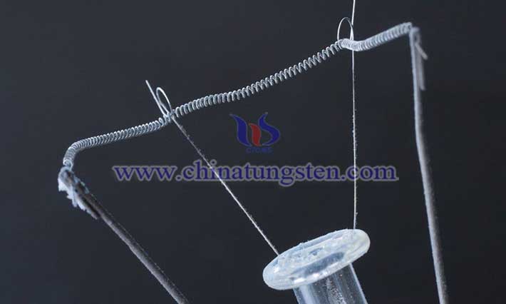
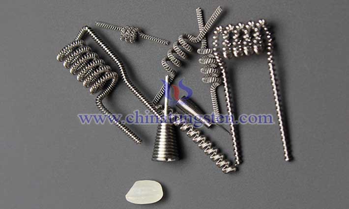
Tungsten wire is formed by cold rolling, hot rolling, extrusion and spin-forging processes of tungsten or tungsten alloy, which owns higher strength and toughness, and it has become one of the most promising candidates for the cutting industry. Tungsten wire is made of metal tungsten bar or doped tungsten bar after draping, forging, and continuous re-drawing. Tungsten wire was invented mainly to solve the problem of traditional incandescent light emitters, but also applied in cutting, heat generation, electrical conductivity and other applications due to its benign hardness and strength. Since its introduction in 1903, most tungsten filaments have been used to make filaments for incandescent, tungsten halogen lamps and electrodes for gas discharge lamps, with a few used as heating materials for high-temperature furnaces, heaters for electron tubes, and reinforcement for composite materials.
4.2 Tungsten-based Wire (Tungsten Core Wire)
In recent years, with the trend of thin wafer cutting in PV industry, tungsten wire has been of great interest due to its finer diameter and better flexibility than traditional saw wire. Since this year, Changsha Dialine New Material, Xiamen Tungsten, Xiamen Tungsten Co. and other industry leaders have been promoting the technical reform and expansion project of tungsten wire for PV, which is intended to capture development prospects of PV industry, semiconductor industry and other areas.
4.3 Tungsten-Based Wire of China Tungsten Online
At the end of 2021, China Tungsten Online (CTOMS) and its team up with industry partners who hold many years of tungsten wire production capacity to conduct testing and research on the suitability of the tungsten-based wire for diamond wire saw. Meanwhile, CTOMS keeps cooperating with diamond wire processors to test the performance of tungsten steel diamond wire saw, and has achieved good test results. Therefore, CTOMS warmly welcomes all walks of life to jointly carry out various means of cooperation.
The traditional tungsten wire information has been uploaded to Tungsten Wire’s web. Parts of the tungsten-based diamond wire saws’ information and markets price will be listed on our news web. Any requirements and willingness for cooperation, please feel free to contact us! zhenghua@ctia.com.cn
For more information about tungsten, tungsten wire and its properties, please visit China Tungsten Industry Association’s (CTIA) web site, or subscribe our official account of Wechat "中钨在线(Chinatungsten)" for getting the latest market information and prices of tungsten and molybdenum materials daily.
In the meantime, China Tungsten will also keep tracking the tungsten-based diamond wire saw and PV cutting information actively and focusing on the information of CTIA GROUP, China Tungsten and Hightech Materials Co., Ltd., and Xiamen Tungsten Co., Ltd. as well as the market price of tungsten-based dimond wire saw.
Chapter 1 of the "Market Research of Tungsten Wire for Diamond Wire Saws in China's Photovoltaic Industry" provides an overview of the main concepts involved tungsten-based diamond wire in the PV industry. It kicks off the ChapterⅡfor keeping up unfolding the overview of the PV industry and the trend of demand for diamond wire.
The "Market Research of Tungsten Wire for Diamond Wire Saws in China's Photovoltaic Industry" is large-scale professional research on tungsten industry initiated by China Tungsten Online. in the first half of 2022. The content covers history, technology, cost and price factors of tungsten-based wire for diamond wire in PV industry.
The research will be updated in our official account "中钨在线(Chinatungsten)" in Wechat. Stay noticed!
For more information, please scan this QR code to follow us

Read/download the full report:
'Market Research of Tungsten Wire for Diamond Wire Saws in China's Photovoltaic Industry'
- Tungsten Manufacturer & Supplier, Chinatungsten Online: www.chinatungsten.com
- Tungsten News & Prices of China Tungsten Industry Association: www.ctia.com.cn
- Molybdenum News & Price: news.molybdenum.com.cn
- Tel.: 86 592 5129696; Fax: 86 592 5129797; Email: sales@chinatungsten.com


 sales@chinatungsten.com