Monocrystal:Sapphire Substrate 1Q14 Price to Increase-LEDforum 2013
- Details
- Category: Tungsten & Sapphire Growth Furnace News
- Published on Friday, 14 February 2014 11:04
- Hits: 2358
The increased demand for sapphire substrates in non LED applications including for smartphone camera lens 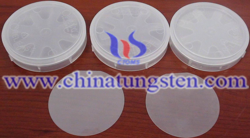 caps plus home button covers, the supply and demand situation has had a turnaround. Sapphire substrate used in smartphones will take up the majority of the production capacity, said Mikhail Berest, Senior VP Global Sales Director, Monocrystal , a large global sapphire substrate manufacturer. It is expected 1Q14 and 2Q14 substrate price will have a large increase of 10 to 15 percent.
Following Apple’s use of sapphire substrate in home buttons in the latest iPhone, industry insiders predict that smartphone manufacturers will soon begin using sapphire substrate in phone displays, said Berest during an interview at LEDforum 2013. Companies that already use sapphire substrate include Apple and LG. Current production capacity demands for 2nch sapphire substrate are about 1.5 to 2 million pieces.
Sapphire substrate for high-end applications is facing a supply shortage of 20 to 30 percent. Rising use of sapphire substrate outside of LEDs provides an opportunity for price increases, said Berest. Following the increase in demand for applications outside of LED, LED chip manufacturers are currently extending the period for sapphire substrate orders.
Sapphire substrate prices will begin increasing10 to 15 percent in 1Q14. Prices are expected to likewise up 10-15 percent in 2Q14, said Berest. Smartphone manufacturers are also expected to begin using sapphire substrate in phone displays in 2014. Launch of new products using sapphire substrate in display screens might cause the next price hike.
Tungsten Manufacturer & Supplier: Chinatungsten Online - http://www.chinatungsten.com
Tel.: 86 592 5129696; Fax: 86 592 5129797
Email: sales@chinatungsten.com
Tungsten & Molybdenum Information Bank: http://i.chinatungsten.com
Tungsten News & Tungsten Prices, 3G Version: http://3g.chinatungsten.com
Molybdenum News & Molybdenum Price: http://news.molybdenum.com.cn
Sapphire Wafer
- Details
- Category: Tungsten & Sapphire Growth Furnace News
- Published on Thursday, 13 February 2014 13:32
- Hits: 2424
Sapphire wafer with complete orientation options including C plane , A plane , R plane and M plane , in 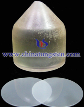 diameter range from 1" to 4" , square substrate is also available as well , size from 10 x 10 mm to 100 x 100 mm . Substrate are produed as per SEMI standards it has good surface finish Ra < 5A and high cleanliness , SWI can offer epi ready grade sapphire wafer for your epitaxial growth . Sapphire wafer are produced by Czochralski method , due to it's high strength, high anti-corrosion high anti-abrasion , low dielectric loss and good electrical insulation , single crystal sapphire wafer plays an increasingly important role as a material for blue LED and high Tc superconductor and microwave applications. Contact us for for further information on price & delivery time .
Thick GaN layers were grown by hydride vapor phase epitaxy (HVPE) with the aim of using these layers as a homoepitaxial substrate to improve device quality of laser diodes or light emitting diodes. HVPE is very useful for thick layer growth since the growth rate can reach from several ten up to one hundred micron per hour. In this experiment, the growth began as selective growth through openings formed in a SiO2 mask. Facets consisting of planes were formed in the early stage and a continuous film developed from the coalescence of these facets on the SiO2 mask. As a result, GaN layers with a dislocation density as low as 6×107 cm-2 were grown on 2-inch-diameter sapphire wafers. These GaN layers were crack-free and had mirror-like surface.
Tungsten Manufacturer & Supplier: Chinatungsten Online - http://www.chinatungsten.com
Tel.: 86 592 5129696; Fax: 86 592 5129797
Email: sales@chinatungsten.com
Tungsten & Molybdenum Information Bank: http://i.chinatungsten.com
Tungsten News & Tungsten Prices, 3G Version: http://3g.chinatungsten.com
Molybdenum News & Molybdenum Price: http://news.molybdenum.com.cn
Template-Free Directional Growth of Single-Walled Carbon Nanotubes on a- And r-Plane Sapphire
- Details
- Category: Tungsten & Sapphire Growth Furnace News
- Published on Thursday, 13 February 2014 11:49
- Hits: 2374
Sapphire is a material of a unique combination of physical, chemical and optical properties, which make it  resistant to high temperature, thermal shock, water and sand erosion, and scratching. It is a superior window material for many IR applications from 3µm to 5µm. C-plane sapphire substrates are widely used to grow III-V and II-VI compounds such as GaN for blue LED and laser diodes, while R-plane sapphire substrates are used for the hetero-epitaxial deposition of silicon for microelectronic IC applications.
We report high-throughput growth of highly aligned single-walled carbon nanotube arrays on a-plane and r-plane sapphire substrates. This is achieved using chemical vapor deposition with ferritin as the catalyst. The nanotubes are aligned normal to the direction for growth on the a-plane sapphire. They are typically tens of micrometers long, with a narrow diameter distribution of 1.34 ± 0.30 nm. In contrast, no orientation was achieved for growth on the c-plane and m-plane sapphire, or when Fe films, instead of ferritin, were used as the catalyst. Such orientation control is likely related to the interaction between carbon nanotubes and the sapphire substrate, which is supported by the observation that when a second layer of nanotubes was grown, they followed the gas flow direction. These aligned nanotube arrays may enable the construction of integrable and scalable nanotube devices and systems.
Tungsten Manufacturer & Supplier: Chinatungsten Online - http://www.chinatungsten.com
Tel.: 86 592 5129696; Fax: 86 592 5129797
Email: sales@chinatungsten.com
Tungsten & Molybdenum Information Bank: http://i.chinatungsten.com
Tungsten News & Tungsten Prices, 3G Version: http://3g.chinatungsten.com
Molybdenum News & Molybdenum Price: http://news.molybdenum.com.cn
AlN Growth on Sapphire Substrate by Ammonia MBE
- Details
- Category: Tungsten & Sapphire Growth Furnace News
- Published on Wednesday, 12 February 2014 11:22
- Hits: 2417
Kinetics of Al2O3 surface nitridation and subsequent growth of AlN films on the sapphire substrate by ammonia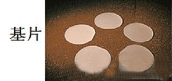 molecular beam epitaxy (MBE) are investigated. Surface morphology evolution during AlN growth is studied in situ by reflection high energy electron diffraction and ex situ by atomic force microscopy. It is found that the surfaces of AlN layers thicker than 100 nm have two major features: a quite smooth background and noticeable amount of hillocks. The influence of growth conditions on the AlN surface morphology is studied in order to find a way for reducing of the hillocks density. A modification of nitridated sapphire surface by small amount of Al (1–2 monolayers) with subsequent treatment of the surface under ammonia flux is proposed. An improvement of AlN surface morphology of the layers grown on the modified surfaces is demonstrated.
Single‐crystal layers of AlN have been grown on sapphire substrates between 1000 and 1100 °C by vapor‐phase reaction of aluminum chlorides with ammonia. The purity, color, crystallinity, growth morphology, and electrical resistivity of the epitaxial layers have been investigated. Infrared specular reflection measurements showed the presence of an appreciable strain at the AlN‐sapphire epitaxy interface. Optical absorption data strongly suggest the AlN is a direct band‐gap material with a value of about 6.2 eV at room temperature.
Tungsten Manufacturer & Supplier: Chinatungsten Online - http://www.chinatungsten.com
Tel.: 86 592 5129696; Fax: 86 592 5129797
Email: sales@chinatungsten.com
Tungsten & Molybdenum Information Bank: http://i.chinatungsten.com
Tungsten News & Tungsten Prices, 3G Version: http://3g.chinatungsten.com
Molybdenum News & Molybdenum Price: http://news.molybdenum.com.cn
GaN Micro-Light-Emitting Diode Arrays with Monolithically Integrated Sapphire Microlenses
- Details
- Category: Tungsten & Sapphire Growth Furnace News
- Published on Wednesday, 12 February 2014 11:13
- Hits: 2419
GaN micro-light-emitting diodes (micro-LEDs) with monolithically integrated microlenses have been  demonstrated. Microlenses, with a focal length of 44 μm and a root mean square roughness of ∼1 nm, have been fabricated on the polished back surface of a sapphire substrate of an array of micro-LEDs by resist thermal reflow and plasma etching. The optical properties of the microlenses have been demonstrated to alter the emission pattern of the LED emitters. The cone of light emitted from this hybrid device is significantly less divergent than a conventional broad-area device. This combination of micro-LED and microlens technologies offers the potential for further improvement in the overall efficiency of GaN-based light emitters.
The fabrication and characterization of a metal semiconductorfield effect transistor (MESFET) based on single crystal GaN. The GaN layer was deposited over sapphire substrate using low pressuremetalorganic chemical vapor deposition. MESFET devices were fabricated on isolated mesas using TiAu for the source and drain ohmic contacts and silver for the gate Schottky. For devices with a gate length of 4 μm (channel opening, i.e., source to drain separation of 10 μm), a transconductance of 23 mS/mm was obtained at −1 V gate bias. Complete pinch‐off was observed for a gate potential of −12 V.
Tungsten Manufacturer & Supplier: Chinatungsten Online - http://www.chinatungsten.com
Tel.: 86 592 5129696; Fax: 86 592 5129797
Email: sales@chinatungsten.com
Tungsten & Molybdenum Information Bank: http://i.chinatungsten.com
Tungsten News & Tungsten Prices, 3G Version: http://3g.chinatungsten.com
Molybdenum News & Molybdenum Price: http://news.molybdenum.com.cn
Plasma Preconditioning of Sapphire Substrate for GaN Epitaxy
- Details
- Category: Tungsten & Sapphire Growth Furnace News
- Published on Tuesday, 11 February 2014 11:13
- Hits: 2394
The crystalline quality of molecular beam epitaxy (MBE)-grown layers of GaN on sapphire strongly depends on 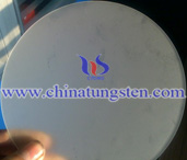 the initial stage of film nucleation and growth. Thus, pre-conditioning of the substrate is of vital importance. We use X-ray photoelectron spectroscopy (XPS) and low energy electron diffraction (LEED) to examine in situ the case for surface cleaning and nitridation of c-plane sapphire substrates upon annealing in UHV and exposure to radio frequency (rf) plasmas of hydrogen and nitrogen, respectively. We find that low temperature (200–300 °C) heat treatment in a hydrogen plasma offers effective removal of adventitious surface contaminants, contrary to annealing in vacuum. Moreover, our XPS data provide unambiguous evidence for formation of surface nitride upon heat treatment in nitrogen plasma at 300–700 °C, in agreement with conclusions inferred from reflection high energy electron diffraction (RHEED). The surface nitride is found to remain stable on subsequent exposure to atmosphere.
Second-harmonic generation in periodically poled GaN by first-order quasiphase matching. The periodically poled structure was grown by plasma-assisted molecular-beam epitaxy. We observed about 9 μW of second-harmonic power from a fundamental input laser wavelength of 1658.6 nm with a normalized conversion efficiency of 12.76% W-1 cm-2. The ability to perform nonlinear wavelength conversion by periodic poling and the fact that GaN has a very wide window of transparency, pave the way for GaN to be used for nonlinear optical devices in telecommunications as well as a nonlinear light source for biochemical detection in the far infrared and deep ultraviolet.
Tungsten Manufacturer & Supplier: Chinatungsten Online - http://www.chinatungsten.com
Tel.: 86 592 5129696; Fax: 86 592 5129797
Email: sales@chinatungsten.com
Tungsten & Molybdenum Information Bank: http://i.chinatungsten.com
Tungsten News & Tungsten Prices, 3G Version: http://3g.chinatungsten.com
Molybdenum News & Molybdenum Price: http://news.molybdenum.com.cn
GaN-Based Light-Emitting Diodes Directly Grown on Sapphire Substrate with Holographically Generated Two-Dimensional Photonic Crystal Patterns
- Details
- Category: Tungsten & Sapphire Growth Furnace News
- Published on Tuesday, 11 February 2014 11:01
- Hits: 2377
As an approach to enhance light extraction from GaN-based light-emitting diodes (LEDs), we inserted a 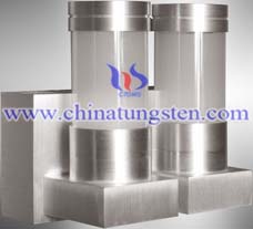 submicron period photonic crystal (PC) pattern at the interface between GaN epilayer and sapphire substrate. A two-dimensional square-lattice pillar array of 600-nm period was produced directly onto the sapphire substrate by a combination of laser holography and inductively-coupled-plasma etching. A standard GaN LED heterostructure was grown on top of the nano-patterned substrate, which was then processed to conventional bottom-emitting LED chips. At the drive current of 20 mA, the PC-LED produced surface-normal output power about 40% higher than that of the reference LED (with no PC integrated). Temperature-dependent photoluminescence measurement indicated that the emission enhancement was solely a structural effect by the integrated PC pattern.
C-plane sapphire substrate misorientation angle on metalorganic chemical vapor deposition of GaN nucleation layers. The angle from c-plane sapphire was varied between 0.05° and 0.30°, tilted towards the m-plane axis. Structural and optical characterization techniques demonstrate an improvement of surface morphology and crystalline quality of GaN nucleation layers as the miscut angle approaches 0.30°. These results correlate well with our previous study of miscut angle on full light-emitting diode structures.
Tungsten Manufacturer & Supplier: Chinatungsten Online - http://www.chinatungsten.com
Tel.: 86 592 5129696; Fax: 86 592 5129797
Email: sales@chinatungsten.com
Tungsten & Molybdenum Information Bank: http://i.chinatungsten.com
Tungsten News & Tungsten Prices, 3G Version: http://3g.chinatungsten.com
Molybdenum News & Molybdenum Price: http://news.molybdenum.com.cn
Effects of Initial Thermal Cleaning Treatment of a Sapphire Substrate Surface on The GaN Epilayer
- Details
- Category: Tungsten & Sapphire Growth Furnace News
- Published on Monday, 10 February 2014 15:24
- Hits: 2533
The effects of the in situ thermalcleaning treatment of a sapphire substrate surface in hydrogenambient on the 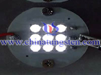 structural, optical, and electrical properties ofepitaxial GaN films grown by metalorganic chemical vapor deposition(MOCVD). Hall effect, X-ray diffraction (XRD), and photoluminescencemeasurements of GaN films grown at 1040°C clearly indicatethat the film quality is strongly affected by the thermal cleaningtreatment of the substrate surface. GaN films under the optimizedthermal cleaning treatment at 1070°C for 10 min showedminimum full-widths at half maximum (FWHMs) of 273 arcsec and728 arcsec for XRD peaks, respectively. In addition,the FWHM of the band-edge emission peak was as narrow as 28.3 meV,and the intensity ratio between the band edge emission and the yellowband emission was as high as 100 at room temperature. It was alsofound that the roughness of sapphire surface was reduced after thethermal treatment.
GaN micro-light-emitting diodes (micro-LEDs) with monolithically integrated microlenses have been demonstrated. Microlenses, with a focal length of 44 μm and a root mean square roughness of ∼1 nm, have been fabricated on the polished back surface of a sapphire substrate of an array of micro-LEDs by resist thermal reflow and plasma etching. The optical properties of the microlenses have been demonstrated to alter the emission pattern of the LED emitters. The cone of light emitted from this hybrid device is significantly less divergent than a conventional broad-area device. This combination of micro-LED and microlens technologies offers the potential for further improvement in the overall efficiency of GaN-based light emitters.
Tungsten Manufacturer & Supplier: Chinatungsten Online - http://www.chinatungsten.com
Tel.: 86 592 5129696; Fax: 86 592 5129797
Email: sales@chinatungsten.com
Tungsten & Molybdenum Information Bank: http://i.chinatungsten.com
Tungsten News & Tungsten Prices, 3G Version: http://3g.chinatungsten.com
Molybdenum News & Molybdenum Price: http://news.molybdenum.com.cn
Epitaxial Growth of ZnO Nanowires on a- And C-Plane Sapphire
- Details
- Category: Tungsten & Sapphire Growth Furnace News
- Published on Monday, 10 February 2014 15:12
- Hits: 2439
Epitaxial ZnO nanowires were grown on a- and c-plane sapphire substrates by metalorganic chemical vapor  deposition without metal catalysts or templates. Nanowires with monodisperse diameters grow in dense arrays perpendicular to a-plane sapphire and with in-plane rotational alignment due to ZnO∥sapphire, View the MathML source epitaxy. On c-plane sapphire, multiple possible epitaxial relations give a mixture of nanowire orientations. The majority of the nanowires grow in one of the three directions all at an angle of 51.8° off the substrate plane with ZnO∥sapphire, View the MathML sourceZnO∥sapphire epitaxy. A small fraction of the nanowires grow perpendicular to the substrate with ZnO∥sapphire.
Optical properties in undoped-ZnO epilayers grown by the laser-molecular-beam epitaxy method on lattice-matched ScAlMgO4 substrates were investigated. The absorption spectrum at 5 K has two sharp peaks, both of which are attributed to resonances of A and B excitons, which reflect a small nonradiative damping constant of excitons as well as high film crystallinity accomplished by the virtue of lattice matching. The coupling strengths of exciton-acoustic phonon and of exciton–longitudinal-optical phonon were directly determined from the temperature dependence of exciton absorption spectra independently for A and B excitons, which are close in energy and obey the same selection rule for each other.
Tungsten Manufacturer & Supplier: Chinatungsten Online - http://www.chinatungsten.com
Tel.: 86 592 5129696; Fax: 86 592 5129797
Email: sales@chinatungsten.com
Tungsten & Molybdenum Information Bank: http://i.chinatungsten.com
Tungsten News & Tungsten Prices, 3G Version: http://3g.chinatungsten.com
Molybdenum News & Molybdenum Price: http://news.molybdenum.com.cn
Uniaxial Locked Epitaxy of ZnO on The A Face of Sapphire
- Details
- Category: Tungsten & Sapphire Growth Furnace News
- Published on Saturday, 08 February 2014 11:59
- Hits: 1206
High-quality, c-oriented ZnO epitaxial films have been grown on the a surface using molecular-beam epitaxy. 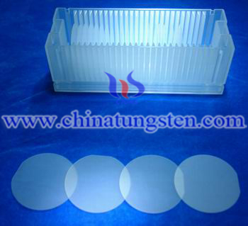 The use of a-oriented sapphire eliminates rotational domains and related structural defects which have limited the use of ZnO in electronic applications. The ZnO epitaxial layers are uniquely oriented with the ZnO/sapphire orientational relationship. This unique orientation is a consequence of the anisotropy of the a-sapphire surface in conjunction with a strong correlation along a single direction leading to the term uniaxial locked epitaxy. High-resolution x-ray diffraction measurements show an increase in x-ray lateral coherence length from several tens of nanometers to ≫0.7 μm for growth of c-oriented ZnO on the a surface as opposed to the c surface of sapphire.
A p-type ZnO was prepared on a sapphire substrate using P2O5 as a phosphorus dopant. As-grown n-type ZnO films doped with phosphorus showed electron concentrations of 1016–1017/cm3 and these films were converted to p-type ZnO by a thermal annealing process at a temperature above 800 °C under a N2 ambient. The electrical properties of the p-type ZnO showed a hole concentration of 1.0×10¹⁷–1.7×10¹⁹/cm3, a mobility of 0.53–3.51 cm2/V s, and a low resistivity of 0.59–4.4 Ω cm. The phosphorus-doped ZnO thin films showed a strong photoluminescence peak at 3.35 eV at 10 K, which is closely related to neutral acceptor bound excitons of the p-type ZnO. This thermal activation process was very reproducible and effective in producing phosphorus-doped p-type ZnO thin films, and the produced p-type ZnO was very stable.
Tungsten Manufacturer & Supplier: Chinatungsten Online - http://www.chinatungsten.com
Tel.: 86 592 5129696; Fax: 86 592 5129797
Email: sales@chinatungsten.com
Tungsten & Molybdenum Information Bank: http://i.chinatungsten.com
Tungsten News & Tungsten Prices, 3G Version: http://3g.chinatungsten.com
Molybdenum News & Molybdenum Price: http://news.molybdenum.com.cn




 sales@chinatungsten.com