Simulation And Analysis of GaN Wafer Bowing on Sapphire Substrate
- Details
- Category: Tungsten & Sapphire Growth Furnace News
- Published on Friday, 28 February 2014 11:15
- Hits: 2621
Using MOCVD (metal-organic chemical vapor deposition) to analyze the growth of GaN-base photoelectric 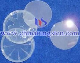 devices on the sapphire substrate is a common method in the semiconductor lighting industry. In recent years, along with the unceasing enhancement of epitaxy technology and related technologies, larger sapphire substrates are needed. The optimization and improvement of MOCVD reaction chamber structure with large-scale epitaxial wafers have been studied by many domestic researchers. Li et al. optimized high-frequency heating graphite base groove structure with eight-inch and twelve-inch substrates. Ying-lu et al.studied the heating modulate curve of radiation heating MOCVD and proposed the design principles of the outer heater. To improve the production efficiency, some great MOCVD manufacturers also focus on how to improve and increase the MOCVD cavity and the sapphire substrate size in foreign countries. At present, two-inch and four-inch epitaxial wafers are frequently used, so manufacturers who can produce six-inch SiC and Si substrate epitaxial wafers with high quality in foreign countries would sell chips abroad.
With the growth of the III-nitrides, sapphire becomes the most extensively used substrate material. Crystals of sapphire with good quality and low price can be easily got. Besides, sapphire is stable at high temperature and the growth technology of nitrides on sapphire is now fairly mature. However, the problem of wafer bowing, which results from the difference in thermal expansion coefficient between GaN epitaxial layer and sapphire, has become much more serious in larger-diameter wafers. It will deteriorate the contact between the substrates and the equipment stages or the subsectors during device process, which will result in degradation in the device uniformity or failures in lithography.
Tungsten Manufacturer & Supplier: Chinatungsten Online - http://www.chinatungsten.com
Tel.: 86 592 5129696; Fax: 86 592 5129797
Email: sales@chinatungsten.com
Tungsten & Molybdenum Information Bank: http://i.chinatungsten.com
Tungsten News & Tungsten Prices, 3G Version: http://3g.chinatungsten.com
Molybdenum News & Molybdenum Price: http://news.molybdenum.com.cn
Morphology of the Surface of modified AlN/Sapphire Substrates Obtained by Thermochemical Nitridation Method
- Details
- Category: Tungsten & Sapphire Growth Furnace News
- Published on Thursday, 27 February 2014 11:25
- Hits: 2473
Sapphire is the material most widely used in the capacity of substrates for technical devices based on the  nitrides GaN, InN, AlN and their solid solutions. However, the method of heteroepitaxy of the nitrides on sapphire substrates results in high dislocation density and other structure defects, due to discrepancy in the crystal lattice parameters and thermal expansion coefficients of these materials. This essentially complicates the obtaining of heterostructures with high functional characteristics. Since the commercial production of the substrates for homoepitaxial growth is expensive, much attention is being paid nowadays to the use of modified sapphire substrates with buffer nitride layers (GaN/sapphire or AlN/sapphire templates) which play the role of inherent nitride quasi-substrates. We have developed a new method for the obtaining of AlN/sapphire templates based on nitridation of sapphire in a gaseous mixture containing N2, СО, СО2, Н2, Н2О with low concentration of СО2 and Н2О.
This method allows to obtain polar AlN//Al2O3, AlN//Al2O3), semipolar (AlN// Al2O3) and nonpolar ( AlN// Al2O3) crystalline AlN layers on the surface of sapphire. Their thickness ranges between 20-30nm and several microns, the rocking curve half-width is less than 1º. In contrast to well-known deposition methods in which epitaxial films are obtained using external source, in the given method AlN layer is formed due to dissolution of nitrogen in anion-deficient corundum followed by crystal-chemical transformations in the surface-adjacent layer of sapphire substrate. Therefore, the nitride layer is to be formed after the stage of corundum reduction followed by etching of the substrate surface. The goal of the present work was to establish regularities of the influence of reducing annealing of sapphire substrate on the morphology of the surface of AlN/sapphire templates.
Tungsten Manufacturer & Supplier: Chinatungsten Online - http://www.chinatungsten.com
Tel.: 86 592 5129696; Fax: 86 592 5129797
Email: sales@chinatungsten.com
Tungsten & Molybdenum Information Bank: http://i.chinatungsten.com
Tungsten News & Tungsten Prices, 3G Version: http://3g.chinatungsten.com
Molybdenum News & Molybdenum Price: http://news.molybdenum.com.cn
2013 Deep Research Report on Global And Chinese Sapphire Substrate Industry
- Details
- Category: Tungsten & Sapphire Growth Furnace News
- Published on Thursday, 27 February 2014 11:11
- Hits: 2440
This 2013 Deep Research Report is a professional and in-depth research report on the Global and Chinese 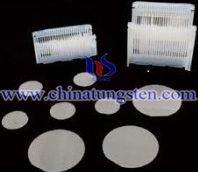 sapphire substrate industry. The report begins by discussing the industry giving details on definition, classification, manufacturing process and product specifications.
The report then examines 17 Global and 12 Chinese manufacturers presenting information on capacity, production cost, selling price, profit, production value, profit margin, products, customers, raw materials and equipment sources.
The report also gives statistics on market shares, production market shares, global and Chinese demand, supply and shortage. It also offers details on price, cost, profit, production values and profit margins. Finally, the report also analyses the 3 million pieces sapphire substrate project feasibility analysis and related research conclusions.
Tungsten Manufacturer & Supplier: Chinatungsten Online - http://www.chinatungsten.com
Tel.: 86 592 5129696; Fax: 86 592 5129797
Email: sales@chinatungsten.com
Tungsten & Molybdenum Information Bank: http://i.chinatungsten.com
Tungsten News & Tungsten Prices, 3G Version: http://3g.chinatungsten.com
Molybdenum News & Molybdenum Price: http://news.molybdenum.com.cn
The Effects of Sapphire Substrates Processes to The LED Efficiency
- Details
- Category: Tungsten & Sapphire Growth Furnace News
- Published on Wednesday, 26 February 2014 14:18
- Hits: 2497
Recently, GaN-based blue and near-UV LEDs are extensively studied in the emerging solid-state lighting 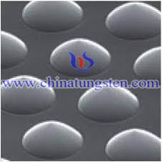 industry as a key technology. The light extraction efficiency (LEE) is very important factor in fabricating high brightness, high efficiency GaN-based light-emitting diode (LED). As well known, the large difference in the refractive index between the GaN(2.40) and air caused a narrow escape cone for the light in GaN crystal. One most used method is roughness or texture on interfaces, such as the patterned sapphire substrate (PSS) recently and the increasing efficiency of PSS LED is considered as a consequence of the light scattering by the PSS. Huang, etc developed the side wall shaping and truncated inverted pyramid (TIP) shaping technology to increase the external quantum efficiency (EQE) of GaN LED.
The flip-chip technology is also wildly studied because of its excellent performance in thermal conductivity and EQE these years. But the influence of sapphire substrate processes in the back-end process is few considered. In this work, the relation between extraction efficiency of GaN-based LED and several parameters of the sapphire substrate is studied, including thickness, roughness and package method. Firstly, the thickness of sapphire substrate in the back-end processes is studied. After choose a better sapphire thickness, we develop the roughness method using just a grinding process and the bottom face periodic pattern by dry etching technique to improve the external quantum efficiency. The different surface structure on the bottom surface of sapphire substrates are analyzed basis on geometry ray tracing simulation, and compared with experiments.
Tungsten Manufacturer & Supplier: Chinatungsten Online - http://www.chinatungsten.com
Tel.: 86 592 5129696; Fax: 86 592 5129797
Email: sales@chinatungsten.com
Tungsten & Molybdenum Information Bank: http://i.chinatungsten.com
Tungsten News & Tungsten Prices, 3G Version: http://3g.chinatungsten.com
Molybdenum News & Molybdenum Price: http://news.molybdenum.com.cn
A Sapphire Substrate Sapphire Semiconductor Products
- Details
- Category: Tungsten & Sapphire Growth Furnace News
- Published on Wednesday, 26 February 2014 14:03
- Hits: 2493
Sapphire semiconductor substrates are manufactured at sapphire products from high quality optical grade 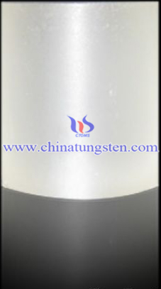 Czochralski sapphire, integrated facilities allow regulation of the production of substrates from crystal growth to fabrication and to accommodate special requests on very short notice.
Sapphire semiconductor substrates are available in all orientations including R-axis (10-12), C-axis (0001), A-axis (11-20), and M-axis (11-10). Substrates are available in various shapes (circular, rectangle, or square), from a few mm up to 100mm in size, and finishes according to customer specification. Primary flats(as per industry standards) are provided on circular substrates for orientation purposes; secondary flats are available on request. Substrate thickness' range from 0.013" (0.25mm) to 0.025" (0.675mm), depending on your particular application requirements.
Tungsten Manufacturer & Supplier: Chinatungsten Online - http://www.chinatungsten.com
Tel.: 86 592 5129696; Fax: 86 592 5129797
Email: sales@chinatungsten.com
Tungsten & Molybdenum Information Bank: http://i.chinatungsten.com
Tungsten News & Tungsten Prices, 3G Version: http://3g.chinatungsten.com
Molybdenum News & Molybdenum Price: http://news.molybdenum.com.cn
LED-on-Si:A Looming Threat for Sapphire Makers
- Details
- Category: Tungsten & Sapphire Growth Furnace News
- Published on Tuesday, 25 February 2014 14:31
- Hits: 2593
All major LED makers are currently exploring opportunities for transitioning from a sapphire-based technology 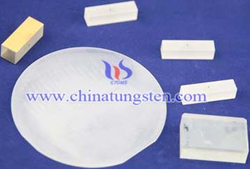 platform to a silicon-based one (“LED-on-Si”); this interest is driven by a potential cost savings of up to 60% at the die level. But while significant progress has been made, the technology still faces hurdles, and it remains to be seen whether the leading proponents of LED-on-Si, like Bridgelux/Toshiba and Lattice Power, will be able to tackle all of the remaining challenges and transition to mass manufacturing in a cost-effective manner. For most other LED companies, LED-on-Si is often an important development axis, but not a necessary milestone on their manufacturing roadmap. The jury is still out, but in the meantime, investments in the large-diameter sapphire platform are often postponed pending the outcome of LED-on-Si.
SoS to Provide Welcome Upsides, But Could Cell Phone Windows Be The Next Killer Application?
The Silicon on Sapphire (SoS) application could represent a nice upside for the happy few that enter the supply chain. Demand more than doubled in 2012 and could do the same in 2013. Leading SoS company Peregrine has developed a compelling Antenna Switch technology that has already achieved vast success in smart phones. The company benefits from strong macro trends in the cell phone market and is developing new components that could further increase not only SoS content per phone, but also wafer demand. Opportunities for these new components (Power Amplifiers and tunable capacitors), as well as for competing technologies developed by companies like Paratek (now part of cell phone maker RIM), may bring new volume applications to sapphire wafer manufacturers.
Tungsten Manufacturer & Supplier: Chinatungsten Online - http://www.chinatungsten.com
Tel.: 86 592 5129696; Fax: 86 592 5129797
Email: sales@chinatungsten.com
Tungsten & Molybdenum Information Bank: http://i.chinatungsten.com
Tungsten News & Tungsten Prices, 3G Version: http://3g.chinatungsten.com
Molybdenum News & Molybdenum Price: http://news.molybdenum.com.cn
Sapphire Substrates Market Forecasts to 2017 in New Research Report
- Details
- Category: Tungsten & Sapphire Growth Furnace News
- Published on Tuesday, 25 February 2014 14:18
- Hits: 2530
The sapphire material shortage experienced from 2010 to early 2011 created a window of opportunity for new  entrants. In the last two years, more than 80 companies announced their intention to enter the industry, bringing the potential number of players to 130+ -- with more than 50 of these potential new entrants located in China. Coupled with slow demand from LED makers in 2012, this has created a very challenging environment with cores and wafers often selling at prices at or below manufacturing cost. Revenues increased 15% in 2011 but are expected to drop 9% in 2012 due to lower Average Selling Prices, despite volume increase and a favorable product mix with the percentage of PSS wafers increasing dramatically. These difficult market conditions will trigger an industry rationalization through consolidation and attrition that should take place in 2013 and 2014; activities that the Yole Finance business unit is monitoring closely. In the long-term, as the environment remains extremely competitive, we expect the industry to evolve toward a more vertically integrated model in order to limit margin stacking. A handful of tier-1 worldwide leaders should emerge from this rationalization, along with smaller tier-2 regional players.
“Sapphire Substrates 2013” presents historical and future price trends for material and finished wafers, as well as a detailed supply/demand analysis. Volume forecasts are presented for material, standard and PSS wafers, along with a revenue forecast for finished wafers.
Tungsten Manufacturer & Supplier: Chinatungsten Online - http://www.chinatungsten.com
Tel.: 86 592 5129696; Fax: 86 592 5129797
Email: sales@chinatungsten.com
Tungsten & Molybdenum Information Bank: http://i.chinatungsten.com
Tungsten News & Tungsten Prices, 3G Version: http://3g.chinatungsten.com
Molybdenum News & Molybdenum Price: http://news.molybdenum.com.cn
Advanced Sappire Single-Wafer Surface Machining
- Details
- Category: Tungsten & Sapphire Growth Furnace News
- Published on Monday, 24 February 2014 14:08
- Hits: 2463
Less sapphire removal is required to eliminate wire saw damage and to achieve good wafer geometry, 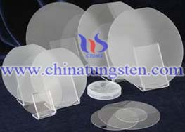 enabling us to start with sapphire blanks that are up to 20% thinner. This results in more wafers per boule and reduces kerf loss. Based on current sapphire costs, this could result in a 20% savings for 4" and a 12% savings for 6" processes.
Wafer yields are much greater since there is never more than one wafer at risk at any time. Improved wafer geometry and better TTV result in more uniform EPI layers and increased die yield, which should result in higher quality, more consistent die -- generating more revenue per wafer for both sapphire substrate and LED manufacturers.
Tungsten Manufacturer & Supplier: Chinatungsten Online - http://www.chinatungsten.com
Tel.: 86 592 5129696; Fax: 86 592 5129797
Email: sales@chinatungsten.com
Tungsten & Molybdenum Information Bank: http://i.chinatungsten.com
Tungsten News & Tungsten Prices, 3G Version: http://3g.chinatungsten.com
Molybdenum News & Molybdenum Price: http://news.molybdenum.com.cn
Understand LED Driver Design And Dimming Techniques That Can Deliver Optimal SSL Products
- Details
- Category: Tungsten & Sapphire Growth Furnace News
- Published on Monday, 24 February 2014 13:57
- Hits: 2381
The driver electronics in a solid-state lighting (SSL) lamp or luminaire are arguably more important for optimal  performance than the LEDs that provide the light. Indeed poor driver design can result in unacceptable flicker, audible noise, electromagnetic emission issues, and many other maladies that make products unacceptable and indeed can give LED lighting a bad reputation. This webcast will examine driver topologies and design techniques that enable high performing products including the capability of dimming smoothly and uniformly.
The presentation will focus on drivers that directly covert the AC line input to the constant-current DC output required to power LEDs. Attendees will learn about a variety of circuit topologies that can be successfully used in SSL products, along with how to match the various topologies to specific application requirements. Moreover the presentation will look at linear and switching techniques for dimming LEDs and discuss the approaches that can deliver flicker-free performance.
Tungsten Manufacturer & Supplier: Chinatungsten Online - http://www.chinatungsten.com
Tel.: 86 592 5129696; Fax: 86 592 5129797
Email: sales@chinatungsten.com
Tungsten & Molybdenum Information Bank: http://i.chinatungsten.com
Tungsten News & Tungsten Prices, 3G Version: http://3g.chinatungsten.com
Molybdenum News & Molybdenum Price: http://news.molybdenum.com.cn
Blackjack Lighting launches Starburst LED chandelier Employing Optical Light Guides
- Details
- Category: Tungsten & Sapphire Growth Furnace News
- Published on Friday, 21 February 2014 11:20
- Hits: 1272
Starburst LED chandelier's laser-cut light guides take LED decorative fixtures in a beautiful new direction.
One of the innovative designs from BlackJack Lighting's 2014 collection, the dramatic Starburst LED chandelier by Stephen Blackman remains true to the company's quest to define and design the next generation of decorative lighting.
BlackJack's new Starburst chandelier fits into a variety of applications once dominated by incandescent chandeliers, yet this high-tech interpretation breaks new ground with its innovative use of optical light guides that optimize LED illumination.
Located at the tip of the fixture's arms, the faceted optical acrylic light guides are laser cut to a sharp, flat edge and coated with a special frosting. Light from tiny LEDs shines into and through the light guides and bounces off of the special coating, sending bright light in a wide, even spread. When the light is turned off, the light guides become diamond-like elements on angular Polished Nickel arms.
STARBURST FEATURES: Triac dimmable * LED pc boards within each arm are easily replaced in the field * Polished Nickel finish * Available in two sizes: 18 inches and 23 inches.
Tungsten Manufacturer & Supplier: Chinatungsten Online - http://www.chinatungsten.com
Tel.: 86 592 5129696; Fax: 86 592 5129797
Email: sales@chinatungsten.com
Tungsten & Molybdenum Information Bank: http://i.chinatungsten.com
Tungsten News & Tungsten Prices, 3G Version: http://3g.chinatungsten.com
Molybdenum News & Molybdenum Price: http://news.molybdenum.com.cn






 sales@chinatungsten.com