Sensing Characteristics of Epitaxially-Grown Tin Oxide Gas Sensor on Sapphire Substrate
- Details
- Category: Tungsten & Sapphire Growth Furnace News
- Published on Friday, 24 January 2014 11:18
- Hits: 2233
Epitaxial SnO2 film was grown on a sapphire substrate using a reactive rf magnetron sputter. The  microstructure of the thin film was investigated using the 3C2 beam line from a Pohang Light Source (PLS) consisting of a 2 GeV electron accelerator, four circle X-ray diffractometer, atomic force microscopy (AFM), and transmission electron microscopy (TEM) comparing with the SnO2 film on the polished alumina. It was confirmed that the thin film grew epitaxially on the sapphire substrate with a variant crystal structure. No grain boundary was exhibited on the surface of the epitaxial thin film. A large portion of the sorption sites in SnO2 films appears to react easily with the gas.
An epitaxial SnO2 gas sensor, with a Pt heater and electrodes, exhibited a high sensitivity to combustible gases and a particular sensitivity of 95% to alcohol at 2000 ppm and 350°C. The sensor also showed a good stability with small baseline drift and fast reaction and recovery times of about 5 and 30 s, respectively.
This experiment confirms the good gas-sensing characteristics of an epitaxially-grown SnO2 gas sensor.
Tungsten Manufacturer & Supplier: Chinatungsten Online - http://www.chinatungsten.com
Tel.: 86 592 5129696; Fax: 86 592 5129797
Email: sales@chinatungsten.com
Tungsten & Molybdenum Information Bank: http://i.chinatungsten.com
Tungsten News & Tungsten Prices, 3G Version: http://3g.chinatungsten.com
Molybdenum News & Molybdenum Price: http://news.molybdenum.com.cn
Alternative Microstructure of GaN Nucleation Layers Grown by Low Pressure Metal-Organic Vapor Phase Epitaxy on Sapphire Substrate
- Details
- Category: Tungsten & Sapphire Growth Furnace News
- Published on Thursday, 23 January 2014 11:21
- Hits: 2448
Predominately hexagonal GaN nucleation layers were grown on sapphire substrate by low pressure metal-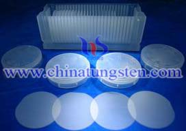
We studied the effects of the growth rate of a GaN buffer layer grown on a GaN epilayer. It was found that this growth rate plays a key role in improving the quality of the GaN film on a sapphire substrate and an optimum growth rate exists that yields the best crystal quality. A GaN film grown on a buffer layer with the optimum growth rate of 18.3 nm/min has an electron Hall mobility of 539 cm2/V s and a dislocation density of approximately 2×108 cm-2. These improvements of GaN film qualities are illustrated by the promotion of the lateral growth mode.
Tungsten Manufacturer & Supplier: Chinatungsten Online - http://www.chinatungsten.com
Tel.: 86 592 5129696; Fax: 86 592 5129797
Email: sales@chinatungsten.com
Tungsten & Molybdenum Information Bank: http://i.chinatungsten.com
Tungsten News & Tungsten Prices, 3G Version: http://3g.chinatungsten.com
Molybdenum News & Molybdenum Price: http://news.molybdenum.com.cn
Growth of Semipolar GaN Layer by Controlling Anisotropic Growth Rates in r-Plane Patterned Sapphire Substrate
- Details
- Category: Tungsten & Sapphire Growth Furnace News
- Published on Thursday, 23 January 2014 11:00
- Hits: 2334
Semipolar GaN was achieved by controlling anisotropic growth rates in a maskless r-plane patterned sapphire 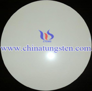 substrate. Upon optimizing the growth conditions, the growth rate of the GaN layer on etched c-plane-like sapphire was much higher than that on other planes such as the original r-plane sapphire. Singularly-oriented GaN was confirmed when GaN was grown on only the c-plane-like sapphire sidewall. The control of the anisotropic growth rate is useful for growing nonpolar and semipolar layers using maskless patterned substrates.
In this letter we describe the structuralcharacteristics of nonpolar a-plane GaNthin filmsgrown on r-plane sapphire substrates via metalorganic chemical vapor deposition. Planar growth surfaces have been achieved and the potential for device-quality layers realized by depositing a low temperature nucleation layer prior to high temperature epitaxialgrowth. The in-plane orientation of the GaN with respect to the -plane sapphire substrate was confirmed to be and This relationship is explicitly defined since the polarity of the -GaN films was determined using convergent beam electron diffraction. Threading dislocations and stacking faults, observed in plan-view and cross-sectional transmission electron microscope images, dominated the -GaN microstructure with densities of and respectively. Submicron pits and crystallographic terraces were observed on the optically specular -GaN surface with atomic force microscopy.
Tungsten Manufacturer & Supplier: Chinatungsten Online - http://www.chinatungsten.com
Tel.: 86 592 5129696; Fax: 86 592 5129797
Email: sales@chinatungsten.com
Tungsten & Molybdenum Information Bank: http://i.chinatungsten.com
Tungsten News & Tungsten Prices, 3G Version: http://3g.chinatungsten.com
Molybdenum News & Molybdenum Price: http://news.molybdenum.com.cn
Alternative Microstructure of GaN Nucleation Layers Grown by Low Pressure Metal-Organic Vapor Phase Epitaxy on Sapphire Substrate
- Details
- Category: Tungsten & Sapphire Growth Furnace News
- Published on Wednesday, 22 January 2014 11:46
- Hits: 2389
Predominately hexagonal GaN nucleation layers were grown on sapphire substrate by low pressure metal-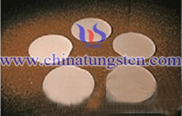 organic vapor phase epitaxy. Tilt angles of GaN single crystallites about the normal of sapphire substrate are determined to be in the range from 0° to 5° by using selected area electron diffraction. A small portion of cubic phase of GaN was observed to be selectively distributed in the grain boundary areas and the instantaneous surface state is suggested to play an important role in the nucleation of the Zincblende phase. Phase transition from hexagonal to cubic GaN caused by heavy radiation from ion beam was also noticed. A critical temperature is proposed to exist in forming predominately cubic or hexagonal GaN nucleation layer.
Epitaxially laterally overgrown GaN on sapphire was used to reduce the number of threading dislocations originating from the interface of the GaN epilayer with the sapphire substrate. The GaN layer above the SiO2 mask area surrounding the window, corresponding to the lateral overgrowth, was nearly free of the threading dislocations. A high density of threading dislocations was observed in the vicinity of GaN grown in the window regions. InGaN multi-quantum-well-structure laser diodes (LDs) grown on pure GaN substrates, which were fabricated by removing the sapphire substrate, were demonstrated. The LDs with an output power of 5 mW exhibited a lifetime of more than 290 h and an estimated lifetime of 10,000 h despite a relatively large threshold current density. The far-field pattern of the LDs with a cleaved mirror facet revealed single-mode emission without any interference effects.
Tungsten Manufacturer & Supplier: Chinatungsten Online - http://www.chinatungsten.com
Tel.: 86 592 5129696; Fax: 86 592 5129797
Email: sales@chinatungsten.com
Tungsten & Molybdenum Information Bank: http://i.chinatungsten.com
Tungsten News & Tungsten Prices, 3G Version: http://3g.chinatungsten.com
Molybdenum News & Molybdenum Price: http://news.molybdenum.com.cn
Nitride-Based High-Power Flip-Chip LED With Double-Side Patterned Sapphire Substrate
- Details
- Category: Tungsten & Sapphire Growth Furnace News
- Published on Wednesday, 22 January 2014 11:12
- Hits: 2300
A nitride-based high-power flip-chip (FC) light-emitting diode (LED) with a double-side patterned sapphire  substrate (PSS) was proposed and realized. Under 350-mA current injection, it was found that forward voltages were 3.24, 3.26, and 3.25 V for the conventional FC LED, FC LED prepared on PSS, and FC LED with double-side PSS, respectively. It was found that the 350-mA LED output powers were 79.3, 98.1, and 121.5 mW for the conventional FC LED, FC LED prepared on PSS, and FC LED with double-side PSS, respectively. In other words, we can enhance the electroluminescence intensity by 53% without increasing operation voltage of the fabricated LED.
An InGaN–GaN light-emitting diode (LED) with a roughened undoped-GaN surface and a silver mirror on the sapphire substrate was fabricated through a double transfer method. It was found that, at an injection current of 20 mA, its luminance intensity was 100% larger than conventional LEDs. Its output power was 49% larger than conventional LEDs.
Tungsten Manufacturer & Supplier: Chinatungsten Online - http://www.chinatungsten.com
Tel.: 86 592 5129696; Fax: 86 592 5129797
Email: sales@chinatungsten.com
Tungsten & Molybdenum Information Bank: http://i.chinatungsten.com
Tungsten News & Tungsten Prices, 3G Version: http://3g.chinatungsten.com
Molybdenum News & Molybdenum Price: http://news.molybdenum.com.cn
Influence of Buffer Layer And Growth Temperature on The Properties of An Undoped GaN Layer Grown on Sapphire Substrate by Metalorganic Chemical Vapor Deposition
- Details
- Category: Tungsten & Sapphire Growth Furnace News
- Published on Tuesday, 21 January 2014 11:40
- Hits: 2296
The influence of low-temperature buffer layer thickness on the electrical properties of GaN film is investigated,  and the surface morphology is also examined by atomic force microscopy. A best surface morphology does not show best electrical properties, which could be attributed to the usual growth mechanism for GaN film on sapphire substrate. The influence of the growth temperature for the final GaN layer is also investigated. When the growth temperature increases to 1100 °C, the mobility is greatly enhanced to 600 cm2/V s with a background carrier density of 3.3×10¹⁶/cm3 at room temperature. The emission energy of the near band gap exciton at a low temperature shows a blueshift with increasing growth temperature due to an enhanced thermal stress. The calculation based on a thermal stress model agrees very well with the photoluminescence measurement. This result could partly explain the reason that the previously published values for the near band gap exciton emission energy are scattered.
Epitaxial GaN layers grown on sapphire contain a very large density of defects (threading dislocations, stacking faults, inversion domain boundaries.Among these defects, we have performed the analysis of the basal stacking faults by high resolution transmission electron microscopy. Two faults, I1 and I2, were identified. The formation of the I1 fault is based on the climb-dissociation process of the (1/3)langle11-20rangle or of the perfect dislocations whereas the I2 fault is due to the shear of the structure leading to a partial dislocation loop.
Tungsten Manufacturer & Supplier: Chinatungsten Online - http://www.chinatungsten.com
Tel.: 86 592 5129696; Fax: 86 592 5129797
Email: sales@chinatungsten.com
Tungsten & Molybdenum Information Bank: http://i.chinatungsten.com
Tungsten News & Tungsten Prices, 3G Version: http://3g.chinatungsten.com
Molybdenum News & Molybdenum Price: http://news.molybdenum.com.cn
High Breakdown Voltage Undoped AlGaN-GaN Power HEMT on Sapphire Substrate And its Demonstration for DC-DC Converter Application
- Details
- Category: Tungsten & Sapphire Growth Furnace News
- Published on Tuesday, 21 January 2014 11:28
- Hits: 2414
Undoped AlGaN-GaN power high electron mobility transistors (HEMTs) on sapphire substrate with 470-V  breakdown voltage were fabricated and demonstrated as a main switching device for a high-voltage dc-dc converter. The fabricated power HEMT realized a high breakdown voltage with a field plate structure and a low on-state resistance of 3.9 mΩ·cm2, which is 10 × lower than that of conventional Si MOSFETs. The dc-dc converter operation of a down chopper circuit was demonstrated using the fabricated device at the input voltage of 300 V. These results show the promising possibilities of the AlGaN-GaN power HEMTs on sapphire substrate for future switching power devices.
SiN-passivated AlGaN/GaN heterojunction FETs (HJFETs) were fabricated on a thinned sapphire substrate. A 16 mm-wide HJFET on a 50 /spl mu/m-thick sapphire exhibited 22.6 W (1.4 W/mm) CW power, 41.9% PAE, and 9.4 dB linear gain at 26 V drain bias. Also, a 32 mm-wide device, measured under pulsed operation, demonstrated 113 W (3.5 W/mm) pulsed power at 40 V drain bias. To our best knowledge, 113 W total power is the highest achieved for GaN on any substrate, establishing the validity of the GaN-on-thinned-sapphire technology.
Tungsten Manufacturer & Supplier: Chinatungsten Online - http://www.chinatungsten.com
Tel.: 86 592 5129696; Fax: 86 592 5129797
Email: sales@chinatungsten.com
Tungsten & Molybdenum Information Bank: http://i.chinatungsten.com
Tungsten News & Tungsten Prices, 3G Version: http://3g.chinatungsten.com
Molybdenum News & Molybdenum Price: http://news.molybdenum.com.cn
Optical Properties of Single-Crystalline ZnO Nanowires on M-Sapphire
- Details
- Category: Tungsten & Sapphire Growth Furnace News
- Published on Monday, 20 January 2014 15:52
- Hits: 2364
ZnO nanowires have been synthesized using a catalyst-assisted heteroepitaxial carbothermal reduction  approach on a m-sapphire substrate. Intricate and uniform arrays have been obtained with each nanowire forming an angle ∼30° with the substrate normal. Photoluminescence studies at room temperature for wavelengths between 335 and 620 nm reveal a strong single exciton peak at ∼380 nm (3.26 eV) with accompanying deep-level blueshifted emission peaks at ∼486, 490, and 510 nm. UV resonant Raman spectroscopy has been used to characterize the nanowires at room temperature with multiphonon scattering exhibiting phonon quantum confinement.
Hydride vapor phase epitaxy (HVPE) was performed to prepare thick GaN films. It is found that (1) surface treatment of the sapphire substrate by the Ga+HCl gas just before the growth of GaN film reduces the pit density and improves the crystalline quality of the epitaxial GaN film(2) the photoluminescence (PL) spectrum measured at 4.2 K shows the free A-exciton line and a narrow I2 line, indicating that the GaN crystals prepared in this study are of high purity and high crystalline quality, and (3) the magnitude of the strain of the homo-epitaxially grown GaN on a thick GaN buffer layer thus prepared is less than half that of a hetero-epitaxially grown GaN on sapphire. These results show that high quality, thick single crystals of GaN can be prepared homo-epitaxially using HVPE.
Tungsten Manufacturer & Supplier: Chinatungsten Online - http://www.chinatungsten.com
Tel.: 86 592 5129696; Fax: 86 592 5129797
Email: sales@chinatungsten.com
Tungsten & Molybdenum Information Bank: http://i.chinatungsten.com
Tungsten News & Tungsten Prices, 3G Version: http://3g.chinatungsten.com
Molybdenum News & Molybdenum Price: http://news.molybdenum.com.cn
A New Method for A Great Reduction of Dislocation Density in A GaN Layer Grown on A Sapphire Substrate
- Details
- Category: Tungsten & Sapphire Growth Furnace News
- Published on Monday, 20 January 2014 15:24
- Hits: 2409
A new method to reduce the dislocation density in a GaN film grown on sapphire substrate by metalorganic  chemical vapor deposition (MOCVD) is reported. In this new method, SiH4 and NH3 gases are simultaneously introduced at a low temperature with a certain time before the growth of an initial low-temperature GaN buffer layer. By transmission electron microscope (TEM), the density of threading dislocation originating from the interface between low-temperature buffer layer and high-temperature GaN layer decreases to be almost invisible from 7×10⁸/cm2 in the conventional MOCVD growth technology for GaN film. Atomic force microscopy indicates that introducing SiH4 and NH3 gases at a low temperature changes surface morphology, which probably enhances the lateral growth and then decreases the dislocation density. This method could be used for fabrication of long-lifetime GaN-based laser instead of epitaxial lateral overgrowth.
N hydride vapor phase epitaxial (HVPE) growth of GaN, the sputtered ZnO layer has been found to be one of the best buffer layers because of the fact that physical properties of ZnO are nearly analogous with those of GaN. With a ZnO buffer layer, the reproducibility of growing GaN single crystal by HVPE has been greatly improved. The GaN films grown by this method show excellent crystalline, electrical, and optical properties. In particular, the Hall mobility of 1920 cm2 V-1 s-1 at 120 K is the highest value that has ever been reported by HVPE.
Tungsten Manufacturer & Supplier: Chinatungsten Online - http://www.chinatungsten.com
Tel.: 86 592 5129696; Fax: 86 592 5129797
Email: sales@chinatungsten.com
Tungsten & Molybdenum Information Bank: http://i.chinatungsten.com
Tungsten News & Tungsten Prices, 3G Version: http://3g.chinatungsten.com
Molybdenum News & Molybdenum Price: http://news.molybdenum.com.cn
Controlled Growth of Zn-Polar ZnO Epitaxial Film by Nitridation of Sapphire Substrate
- Details
- Category: Tungsten & Sapphire Growth Furnace News
- Published on Friday, 17 January 2014 13:45
- Hits: 1223
Surface nitridation is used to eliminate O-polar inversion domains and control the growth of single-domain  Zn-polar ZnO film on sapphire substrate by rf-plasma-assisted molecular-beam epitaxy. It is found that the nitridation temperature is crucial for achieving quality AlN buffer layers and ZnO films with cation polarity, as demonstrated by ex situ transmission electron microscopy. Under optimal growth conditions, a 4×4 surface reconstruction was observed, which is confirmed to be a characteristic surface structure of the Zn-polar films, and can be used as a fingerprint to optimize the ZnO growth.
The properties of 1.2 μm thick GaN films were found to be significantly influenced by the duration of exposing the sapphire substrate to ammonia prior to the GaN growth initiation. The different nitridation schemes of sapphire strongly affect the dislocation structure of GaN films resulting in a decrease of the dislocation density from 2×10¹⁰ to 4×108 cm-2 for shorter NH3 preflow times. Room‐ and low‐temperature electron transport characteristics of these films are specifically affected by the dislocation structure. A 300 K electron mobility as high as 592 cm2/V s was obtained for a short ammonia preflow whereas a long nitridation caused the mobility to drop to 149 cm2/V s. Additionally, the photoluminescence quality deteriorates for samples with a long sapphire nitridation time.
Tungsten Manufacturer & Supplier: Chinatungsten Online - http://www.chinatungsten.com
Tel.: 86 592 5129696; Fax: 86 592 5129797
Email: sales@chinatungsten.com
Tungsten & Molybdenum Information Bank: http://i.chinatungsten.com
Tungsten News & Tungsten Prices, 3G Version: http://3g.chinatungsten.com
Molybdenum News & Molybdenum Price: http://news.molybdenum.com.cn




 sales@chinatungsten.com