Annealing Effects of Sapphire Substrate on Properties of ZnO Films Grown by Magnetron Sputtering
- Details
- Category: Tungsten & Sapphire Growth Furnace News
- Published on Friday, 03 January 2014 11:13
- Hits: 2261
The annealing effects of sapphire substrates on the quality of epitaxial ZnO films grown by dc reactive 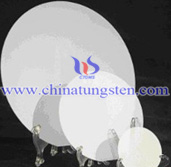 magnetron sputtering were studied. The atomic steps formed on sapphire (α-Al2O3) substrates surface by annealing at high temperature were analyzed by atomic force microscopy. Their influence on the growth of ZnO films was examined by X-ray diffraction and photoluminescence measurements. Experimental results indicate that the film quality is strongly affected by annealing treatment of the sapphire substrate surface. The optimum annealing temperature of sapphire substrates for ZnO grown by magnetron sputtering is 1400 °C for 1 h in air.
Vertically aligned single-crystal ZnO nanorods have been successfully fabricated on semiconducting GaN, Al0.5Ga0.5N, and AlN substrates through a vapor−liquid−solid process. Near-perfect alignment was observed for all substrates without lateral growth. Room-temperature photoluminescence measurements revealed a strong luminescence peak at 378 nm. This work demonstrates the possibility of growing heterojunction arrays of ZnO nanorods on AlxGa1-xN, which has a tunable band gap from 3.44 to 6.20 eV by changing the Al composition from 0 to 1, and opens a new channel for building vertically aligned heterojunction device arrays with tunable optical properties and the realization of a new class of nanoheterojunction devices.
Tungsten Manufacturer & Supplier: Chinatungsten Online - http://www.chinatungsten.com
Tel.: 86 592 5129696; Fax: 86 592 5129797
Email: sales@chinatungsten.com
Tungsten & Molybdenum Information Bank: http://i.chinatungsten.com
Tungsten News & Tungsten Prices, 3G Version: http://3g.chinatungsten.com
Molybdenum News & Molybdenum Price: http://news.molybdenum.com.cn
Visible Lasing from GaN:Eu Optical Cavities on Sapphire Substrates
- Details
- Category: Tungsten & Sapphire Growth Furnace News
- Published on Thursday, 02 January 2014 11:40
- Hits: 2155
We report visible (red) lasing emission from Eu-doped GaN thin films grown on sapphire substrates. The edge 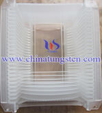 emission fulfills the requirements of stimulated emission properties: super-linear characteristic, spectrum line narrowing, polarization effect, lifetime reduction, and longitudinal modes in a Fabry–Perot cavity. The GaN:Eu active layer has low threshold (∼10 kW/cm2) for the onset of lasing. The optical gain and loss are of the order of 50 and 20 cm−1, respectively. Growth conditions are investigated for gain enhancement and loss reduction. To obtain the high gain and low loss active layer, N-rich growth conditions are required. Channel waveguide cavities result in 5× increase in gain value compared to planar waveguides.
GaN films were grown on sapphire by molecular beam epitaxy (MBE). Two sources of activated nitrogen were investigated: an electron cyclotron resonance (ECR) plasma, and hydrogen azide (HN3). With the ECR plasma source, typical growth rates were ∼ 0.1 μm/h. Films grown in this manner showed significant surface damage from ions, and little if any photoluminescence. With HN3, growth rates were ∼ 0.25 μm/h. Azide-grown films showed smooth surfaces, and sharp band-to-band photoluminescence. This is the first reported use of HN3 to grow III–V nitrides by MBE, and it shows great promise as a nitrogen source.
Tungsten Manufacturer & Supplier: Chinatungsten Online - http://www.chinatungsten.com
Tel.: 86 592 5129696; Fax: 86 592 5129797
Email: sales@chinatungsten.com
Tungsten & Molybdenum Information Bank: http://i.chinatungsten.com
Tungsten News & Tungsten Prices, 3G Version: http://3g.chinatungsten.com
Molybdenum News & Molybdenum Price: http://news.molybdenum.com.cn
Verneuil Method for Growing Sapphire Crystals
- Details
- Category: Tungsten & Sapphire Growth Furnace News
- Published on Thursday, 02 January 2014 11:13
- Hits: 2725
In the Verneuil sapphire crystal growth system, the alumina powder is molten during its fall into an oxygen-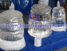 hydrogen flame. The liquid droplets fall on the top of the slowly-pulled crystal. From a physical point of view, the Verneuil process is complex because of the coupling of the turbulent combustion between hydrogen and oxygen, the hydrodynamics of the gas phase and the heat transport by convection, conduction and radiation.
Numerical simulations of the Verneuil crystal growth process have been carried out using the FIDAP finite element software, and the results have been presented in a previous paper. In order to determine the effect of the transparency of the sapphire, some assumptions were used: the process is considered in quasi-steady state, the model is axi-symmetric and the latent heat of fusion is negligible, i.e. the powder is not included in the model. The results obtained in the case where the crystal is considered as opaque have been compared with the simulation of a fully transparent material. Numerical simulation of heat transfer in transparent and semitransparent crystal growth processes.
The transparent crystal appears to be cooler than the opaque one, because in a transparent body the absorption of heat is reduced. The axial thermal gradient in the opaque crystal is smaller than that calculated in the case of a transparent crystal. By comparing the numerical results with experimental thermocouple data, it has been concluded that the simulation of a fully transparent sapphire crystal is more realistic than that of an opaque one.
A further step in this study will be to analyse the effect of the participating media radiation through the sapphire.
Vertical Bridgman method for growing fluoride crystals.
Tungsten Manufacturer & Supplier: Chinatungsten Online - http://www.chinatungsten.com
Tel.: 86 592 5129696; Fax: 86 592 5129797
Email: sales@chinatungsten.com
Tungsten & Molybdenum Information Bank: http://i.chinatungsten.com
Tungsten News & Tungsten Prices, 3G Version: http://3g.chinatungsten.com
Molybdenum News & Molybdenum Price: http://news.molybdenum.com.cn
Two-Dimensional Large-Size Y Ba2Cu3O7 Films (30 × 10 cm2) on CeO2-Buffered Sapphire by A Coating Pyrolysis Process
- Details
- Category: Tungsten & Sapphire Growth Furnace News
- Published on Tuesday, 31 December 2013 15:09
- Hits: 2231
Large-size, two-dimensional Y Ba2Cu3O7 (YBCO) films were successfully prepared by a chemical solution- based coating pyrolysis (CP) process on 30 × 10 cm2 R-plane sapphire substrates with a vacuum-deposited CeO2 buffer layer. The CeO2 layer was very smooth and uniform with an average roughness (Ra) of 0.48 nm by atomic force microscopic observations and highly-oriented by large-area x-ray diffraction θ–2θ scans. The c-axis-oriented YBCO films were prepared by a CP process using a fluorine-free, metal acetylacetonate-based coating solution. A 30 × 10 cm2-rectangular c-axis-oriented YBCO film annealed in a large-diameter tube furnace demonstrated high inductive-Jc values, for which the distribution was fairly uniform, with an average 1.0 MA cm−2 at 77 K.
Epitaxial Naβ″-Al2O3 single crystal films have been grown into sapphire substrates. The kinetic measurements and calculation indicate that the β″-Al2O3 crystal is formed via chemical reactions between the gaseous alkali-species and sapphire substrate which are controlled by diffusion of oxygen species in the solid phase. The mechanism and crystallographic translations of film-growth are discussed.
Tungsten Manufacturer & Supplier: Chinatungsten Online - http://www.chinatungsten.com
Tel.: 86 592 5129696; Fax: 86 592 5129797
Email: sales@chinatungsten.com
Tungsten & Molybdenum Information Bank: http://i.chinatungsten.com
Tungsten News & Tungsten Prices, 3G Version: http://3g.chinatungsten.com
Molybdenum News & Molybdenum Price: http://news.molybdenum.com.cn
Structural Properties of ZnO Grown on GaN ∕ Sapphire Templates The Transition from Nanorods to Thin Films
- Details
- Category: Tungsten & Sapphire Growth Furnace News
- Published on Tuesday, 31 December 2013 14:49
- Hits: 2296
ZnO nanorods were synthesized on formula /sapphire substrates using a modified thermal-evaporation 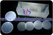 process. The as-synthesized Formula nanorods and thin films were characterized using scanning electron microscopy, micro-Raman, and X-ray diffraction techniques. The morphology of the Formula changes from nanorods to continuous thin films when the growth temperature increases to 800°C. Further increase in the growth temperature leads to a lower growth rate of Formula along the direction. Micro-photoluminescence measurements show ultraviolet band-edge emission peaks around Formula from both nanorods and thin films. Realization of such Formula structures may be useful for the fabrication of hybrid Formula optoelectronic devices.
Recent results suggests that Formula may be a p‐type transparent conductor, but thin film synthesis is difficult because of the complex Formula phase diagram. We report a robust method of making c‐axis oriented Formula thin films. Thin film precursors of formula were deposited on sapphire substrates by radio‐frequency sputtering and by pulsed‐laser deposition. Subsequent annealing in air at Formula in a closed crucible containing Formula and Formula powders yielded nearly phase‐pure, biaxially textured Formula . The film were p‐type and transparent with a gap of Formula .
Tungsten Manufacturer & Supplier: Chinatungsten Online - http://www.chinatungsten.com
Tel.: 86 592 5129696; Fax: 86 592 5129797
Email: sales@chinatungsten.com
Tungsten & Molybdenum Information Bank: http://i.chinatungsten.com
Tungsten News & Tungsten Prices, 3G Version: http://3g.chinatungsten.com
Molybdenum News & Molybdenum Price: http://news.molybdenum.com.cn
Synthesis of Horizontally-Aligned Single-Walled Carbon Nanotubes With Controllable Density on Sapphire Surface And Polarized Raman Spectroscopy
- Details
- Category: Tungsten & Sapphire Growth Furnace News
- Published on Monday, 30 December 2013 14:28
- Hits: 2241
The facile synthesis of aligned single-walled carbon nanotube (SWNT) arrays with controllable density on  A-face sapphire substrates and the measurement of their polarized Raman spectra. The catalyst was prepared by simply dipping the sapphire substrate into a mixed solution of iron nitrate and molybdenum acetate, where Mo improved the nanotube yield as well as reproducibility. The angle dependence of the Raman spectra measured for the high-density nanotube array indicated the growth of SWNTs aligned mainly in the View the MathML source direction and two other directions. This suggests multiple mechanisms for the alignment, such as the pseudo one-dimensional Al arrangement and the presence of shallow grooves.
The conditions for obtaining CdSe epitaxial layers on sapphire substrates with orientation are described. The sublimation of polycrystalline CdSe and its oriented deposition on the substrates is carried out in a localized quasiclosed volume of a vacuum system. The temperature influence on the structure and morphology of deposited layers is investigated in the crystallization region.
Tungsten Manufacturer & Supplier: Chinatungsten Online - http://www.chinatungsten.com
Tel.: 86 592 5129696; Fax: 86 592 5129797
Email: sales@chinatungsten.com
Tungsten & Molybdenum Information Bank: http://i.chinatungsten.com
Tungsten News & Tungsten Prices, 3G Version: http://3g.chinatungsten.com
Molybdenum News & Molybdenum Price: http://news.molybdenum.com.cn
Extraordinary Alignment of Nb Films with Sapphire And The Effects of Added Hydrogen
- Details
- Category: Tungsten & Sapphire Growth Furnace News
- Published on Monday, 30 December 2013 13:58
- Hits: 2394
The current method of growing large-area graphene on polycrystalline Cu surfaces (foils or thin films) and its  transfer to arbitrary substrates is technologically attractive. However, the quality of graphene can be improved significantly by growing it on single-crystal Cu surfaces. Here we show that high quality, large-area graphene can be grown on epitaxial single-crystal Cu thin films on reusable basal-plane sapphire substrates for transfer to another substrate. While enabling graphene growth on Cu single-crystal surfaces, this method has the potential to avoid the high cost and extensive damage to graphene associated with sacrificing bulk single-crystal Cu during graphene transfer.
We present the results of high-resolution x-ray scattering studies of the structural coherence of niobium films grown by molecular-beam epitaxy on sapphire substrates. In transverse scans of the out-of-plane Bragg peak we find two components, the sharper of which implies mosaicities an order of magnitudes better than bulk single-crystal Nb, and transverse structural coherence lengths exceeding 104 Å. In addition, we observe that the planes associated with the sharp component are exactly aligned with the sapphire planes. Upon hydrogen loading of the Nb film, we find evidence for a dramatic increase of the lateral coherence length.
Tungsten Manufacturer & Supplier: Chinatungsten Online - http://www.chinatungsten.com
Tel.: 86 592 5129696; Fax: 86 592 5129797
Email: sales@chinatungsten.com
Tungsten & Molybdenum Information Bank: http://i.chinatungsten.com
Tungsten News & Tungsten Prices, 3G Version: http://3g.chinatungsten.com
Molybdenum News & Molybdenum Price: http://news.molybdenum.com.cn
Homoepitaxial Growth of AlN on Nitrided Sapphire by LPE Method Using Ga–Al Binary Solution
- Details
- Category: Tungsten & Sapphire Growth Furnace News
- Published on Friday, 27 December 2013 11:26
- Hits: 2383
A novel liquid phase epitaxy method was proposed for growing an AlN layer using Ga–Al binary flux under 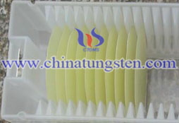 normal pressure. In this method, nitrogen gas was injected into the flux. Then a nitrided sapphire substrate was used as a template to achieve homoepitaxial growth. Advantages of using a nitrided sapphire substrate were demonstrated; the optimum flux composition was investigated. We grew 1-µm-thick c-axis oriented AlN layer for 5 h at 1573 K. The full width at half maximum values of X-ray rocking curves for AlN and were, respectively, 50 and 590 arcsec. Moreover, the surface morphology and interfacial structure were observed using a scanning electron microscope, laser microscope, and high-resolution transmission electron microscope.
By applying conventional epitaxial crystal growth techniques to this VLS process, it is possible to gain precise orientation control during nanowire growth. The technique, vapor-liquid-solid epitaxy (VLSE), is particularly powerful in the controlled synthesis of high-quality nanowire arrays and single-wire devices. For example, ZnO prefers to grow along the direction and readily forms highly oriented arrays when epitaxially grown on an a-plane sapphire substrate . A similar level of growth control can be achieved for GaN10 and Si/Ge systems. It is possible to use this VLSE technique for the growth of nanowire arrays with tight control over size (diameter < 20 nm) and uniformity (< ±10%). In addition, we have explored different types of nanowire heterostructures, including coaxial15 and longitudinal variations. Semiconductor heterostructures enable the confinement of electrons and holes, the guiding of light, and the modulation of both phonon transport and carrier mobility. This size monodispersity and heterostructure control is crucial for many proposed applications for these nanowire arrays, including light emission and field-effect transistors.
Tungsten Manufacturer & Supplier: Chinatungsten Online - http://www.chinatungsten.com
Tel.: 86 592 5129696; Fax: 86 592 5129797
Email: sales@chinatungsten.com
Tungsten & Molybdenum Information Bank: http://i.chinatungsten.com
Tungsten News & Tungsten Prices, 3G Version: http://3g.chinatungsten.com
Molybdenum News & Molybdenum Price: http://news.molybdenum.com.cn
Nanostructured Sapphire Vicinal Surfaces as Templates for The Growth of Self-Organized Oxide Nanostructures
- Details
- Category: Tungsten & Sapphire Growth Furnace News
- Published on Friday, 27 December 2013 11:00
- Hits: 2268
Vicinal substrates of sapphire with miscut angle of 10° from the planes towards the direction have been 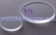 annealed in air in the range from 1000 to 1500 °C. The behaviour of these surfaces has been characterized as a function of the temperature and the thermal treatment time by Atomic Force Microscopy observations. A thermal treatment at 1250 °C allows to stabilize a surface made of periodically spaced nanosized step-bunches. Such stepped surfaces were used as template to grow self-patterned epitaxial oxide nanoparticles by thermal annealing of yttria-stabilized zirconia thin films produced by sol–gel dip-coating. Grazing Incidence Small Angle X-ray Scattering and High-Resolution Transmission Electron Microscopy were used to study the morphology of the nanoparticles and their epitaxial relationships with the substrate.
Crystallization behaviors of sol—gel-derived LiNbO3 films, on sapphire and on MgO-doped LiNbO3 substrate, were observed by in situ TEM and high-resolution TEM. It was found that heterogeneous nucleation and growth of the crystalline LiNbO3 occurred with epitaxy on the interfaces between the films and the substrates, and the resulting epitaxial films were formed by coalescence of the crystallites. The difference in the crystallization behaviors, further, was observed between the films on the substrates. On MgO-doped LiNbO3 substrate which has small lattice mismatch with the film, the nucleation arose easily and the crystallites grew along the interface and towards a surface of the film. However, on sapphire substrate with the large lattice mismatch, the crystallites predominantly grew towards the surface of the film. The resulting film on sapphire substrate contained a large amount of structural defect at the grain boundary. The difference in the crystallization behaviors were discussed.
Tungsten Manufacturer & Supplier: Chinatungsten Online - http://www.chinatungsten.com
Tel.: 86 592 5129696; Fax: 86 592 5129797
Email: sales@chinatungsten.com
Tungsten & Molybdenum Information Bank: http://i.chinatungsten.com
Tungsten News & Tungsten Prices, 3G Version: http://3g.chinatungsten.com
Molybdenum News & Molybdenum Price: http://news.molybdenum.com.cn
Simulation Analysis on the SAPMAC Crystal Growth Process of Large Size Sapphire
- Details
- Category: Tungsten & Sapphire Growth Furnace News
- Published on Thursday, 26 December 2013 11:18
- Hits: 1197
The SAPMAC(sapphire growth technique with micro-pulling and shoulder at cooled center) process has  investigated by numerical simulation method.The characteristics of several different crystal growth stages have been analyzed and compared with Czochralski method,temperature gradient technique and bridgman technique etc.Base on the results of simulation and techniques of different crystal growth stages,the system and control techniques of crystal growth were improved;the conventional SAPMAC furnace was modified with the heat dissipation parameters increased,the heating temperature decreased,the temperature falling curve improved,the additional axial and radial temperature gradient adjusted,so the necking-down,shoulder-extending,iso-diameter and tailing process of the crystal growth can be controlled.The experiment results testified that the grown crystal has better quality and larger size by the improved system of crystal growth and control techniques.
The goal of the research presented here is to apply a global analysis of an inductively heated Czochralski furnace for a real sapphire crystal growth system and predict the characteristics of the temperature and flow fields in the system. To do it, for the beginning stage of a sapphire growth process, influence of melt and gas convection combined with radiative heat transfer on the temperature field of the system and the crystal-melt interface have been studied numerically using the steady state two-dimensional finite element method. For radiative heat transfer, internal radiation through the grown crystal and surface to surface radiation for the exposed surfaces have been taken into account. The numerical results demonstrate that there are a powerful vortex which arises from the natural convection in the melt and a strong and large vortex that flows upwards along the afterheater side wall and downwards along the seed and crystal sides in the gas part. In addition, a wavy shape has been observed for the crystal-melt interface with a deflection towards the melt.
Tungsten Manufacturer & Supplier: Chinatungsten Online - http://www.chinatungsten.com
Tel.: 86 592 5129696; Fax: 86 592 5129797
Email: sales@chinatungsten.com
Tungsten & Molybdenum Information Bank: http://i.chinatungsten.com
Tungsten News & Tungsten Prices, 3G Version: http://3g.chinatungsten.com
Molybdenum News & Molybdenum Price: http://news.molybdenum.com.cn





 sales@chinatungsten.com