The Sapphire Substrate of Aluminum Nitride Buffer Layer of The Prior Art
- Details
- Category: Tungsten & Sapphire Growth Furnace News
- Published on Thursday, 19 December 2013 09:51
- Hits: 2447
The sapphire substrate of aluminum nitride buffer layer such prior art reference discloses a description by which 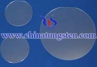 the p-type conductivity in the creation of manufacturing a group III nitride semiconductor laser is (AlxGayIn1 - x-yN, including the case of x = 0, Y = 0 and X = Y = 0), by exposure to electron beams. Such a semiconductor laser having formed thereon, in turn, covered with the group III nitride compound semiconductor (AlxGayIn1 - x-yN Sapphire pn heterojunction of the aluminum nitride substrate a buffer layer; including the case x = 0 Next, Y = 0 and x = Y = 0).
In Japanese Unexamined Patent Publication proposed laser diode (closed) Hei-4 - 242985 is a gallium nitride-based compound semiconductor ((the Al x Ga-X) yIn1-YN; 0 ≤ X ≤ 1, 0 ≤ Y ≤ 1), the impurity-doped active layer used.
Tungsten Manufacturer & Supplier: Chinatungsten Online - http://www.chinatungsten.com
Tel.: 86 592 5129696; Fax: 86 592 5129797
Email: sales@chinatungsten.com
Tungsten & Molybdenum Information Bank: http://i.chinatungsten.com
Tungsten News & Tungsten Prices, 3G Version: http://3g.chinatungsten.com
Molybdenum News & Molybdenum Price: http://news.molybdenum.com.cn
Group III Nitride-Based Compound Semiconductor Layer on A Sapphire Substrate
- Details
- Category: Tungsten & Sapphire Growth Furnace News
- Published on Wednesday, 18 December 2013 11:11
- Hits: 2466
A laser diode made of a Group III nitride based compound semiconductor layers comprising a sapphire 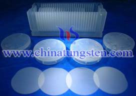
The improved laser diode is made of a gallium nitride base compound semiconductor ((AlxGa1-x)yIn1-yN; 0</=x</=1; 0</=y</=1) with a double heterojunction structure having the active layer held between layers having a greater band gap, the laser diode comprises mirror surfaces formed by cleaving said multi-layered coating and said sapphire substrate in directions parallel to &Lang&0001&Rang& (c axis) of said sapphire substrate. Further, in the improved process, only the intermediate zinc oxide (ZnO) layer is removed by wet etching with a ZnO-selective liquid etchant so as to form gaps between the sapphire substrate and the bottommost sub-layer of said semiconductor laser element layer; and said semiconductor laser element layer is cleaved with the aid of said gaps 20, with the resulting planes of cleavage being used as the mirror surfaces of the laser cavity.
Tungsten Manufacturer & Supplier: Chinatungsten Online - http://www.chinatungsten.com
Tel.: 86 592 5129696; Fax: 86 592 5129797
Email: sales@chinatungsten.com
Tungsten & Molybdenum Information Bank: http://i.chinatungsten.com
Tungsten News & Tungsten Prices, 3G Version: http://3g.chinatungsten.com
Molybdenum News & Molybdenum Price: http://news.molybdenum.com.cn
Growth and Characterization of Nonpolar Zn1−xMgxO (0 ≤ x ≤ 0.113) Epitaxial Films: A Comparison of γ-LiAlO2 and Sapphire Substrates
- Details
- Category: Tungsten & Sapphire Growth Furnace News
- Published on Wednesday, 18 December 2013 10:51
- Hits: 2467
γ-LiAlO2 and sapphire substrates have been employed to grow nonpolar Zn1−xMgxO films using metalorganic  chemical vapor deposition. Zn1−xMgxO films with various Mg contents (0 ≤ x ≤ 0.113) are obtained by adjusting the partial pressure of the Mg metalorganic precursor in gas phase. Mg atoms incorporate within the films by means of substituting Zn. No segregated phase such as MgO or metal Mg is observed throughout the Zn1−xMgxO films. Structural characterization of the films indicates that γ-LiAlO2 is a superior substrate to sapphire for the growth of the nonpolar Zn1−xMgxO films.
The epitaxial Zn1−xMgxO films are successfully grown on the γ-LiAlO2 substrates with the epitaxial relationship of ZMO LAO. On the other hand, the Zn1−xMgxO films with both and orientations are obtained on sapphire substrates although Zn1−xMgxO becomes dominant with increasing Mg content. In addition, room-temperature cathodoluminescence spectra of the epitaxial Zn1−xMgxO films show an obvious blue shift of the near-band-edge emission with increasing Mg content, demonstrating bandgap engineering in the epitaxial nonpolar Zn1−xMgxO films on the γ-LiAlO2 substrates.
Tungsten Manufacturer & Supplier: Chinatungsten Online - http://www.chinatungsten.com
Tel.: 86 592 5129696; Fax: 86 592 5129797
Email: sales@chinatungsten.com
Tungsten & Molybdenum Information Bank: http://i.chinatungsten.com
Tungsten News & Tungsten Prices, 3G Version: http://3g.chinatungsten.com
Molybdenum News & Molybdenum Price: http://news.molybdenum.com.cn
Synthesis of Single Crystalline GaN Nanoribbons on Sapphire Substrates
- Details
- Category: Tungsten & Sapphire Growth Furnace News
- Published on Tuesday, 17 December 2013 09:59
- Hits: 2342
In previous studies about the synthesis of GaN 1D nanostructures and Ga2O3 only appeared as one of the  components of Ga source. Herein, we have successfully synthesized bulk-quantity GaN nanoribbons on sapphire substrates, from the direct reaction of sputtered Ga2O3 thin films with flowing ammonia. Neither metal catalysts nor templates were used in this process. The detailed characterization of the synthesized ribbon-like 1D nanostructures revealed that they were single crystalline hexagonal wurtzite GaN.
Single crystalline GaN nanoribbons were synthesized through nitriding Ga2O3 thin films deposited on sapphire substrates by radio frequency magnetron sputtering. The component and structure of nanoribbons were investigated by X-ray diffraction (XRD), scanning electron microscopy (SEM), energy-dispersive X-ray (EDX), transmission electron microscopy (TEM) and high-resolution transmission electron microscopy (HRTEM). The flat and smooth ribbon-like nanostructures are high quality single crystalline hexagonal wurtzite GaN. The thickness and width-to-thickness ratio of the grown GaN nanoribbons are in the range of 8–15 nm and ∼5–10, respectively.
Tungsten Manufacturer & Supplier: Chinatungsten Online - http://www.chinatungsten.com
Tel.: 86 592 5129696; Fax: 86 592 5129797
Email: sales@chinatungsten.com
Tungsten & Molybdenum Information Bank: http://i.chinatungsten.com
Tungsten News & Tungsten Prices, 3G Version: http://3g.chinatungsten.com
Molybdenum News & Molybdenum Price: http://news.molybdenum.com.cn
Multiple Growth of Profiled Sapphire Crystals
- Details
- Category: Tungsten & Sapphire Growth Furnace News
- Published on Tuesday, 17 December 2013 09:41
- Hits: 2433
Pulling of shaped sapphire crystals using resistance heating implemented by means of heating elements in a  “circular” or a “linear” growth arrangement is described. The growth equipment can be easily disassembled beacause the individual molybdenum dies are connected to a die-holding block with a diffusion Mo-Mo bonding having a reduced strength. Advantages of the individual processes are described and the influence of the die-top temperature upon the quality of pulled crystal shapes is mentioned.
Edge Defined film Fed Growth (EFG) SaphikonTM sapphire crystals have been grown and successfully processed into windows measuring 225 x 325 mm with a thickness of 5.6 mm. More than 40 windows have been completed and assembled into customer hardware and delivered. The polished and coated windows have exhibited average transmission >93% from 1 to 5 mm and wavefront measurements of <0.1 waves rms (@ 0.633 μm) over a 125 mm aperture. Optical measurement data are presented and aspects of the crystal growth and polishing processes are discussed.
Tungsten Manufacturer & Supplier: Chinatungsten Online - http://www.chinatungsten.com
Tel.: 86 592 5129696; Fax: 86 592 5129797
Email: sales@chinatungsten.com
Tungsten & Molybdenum Information Bank: http://i.chinatungsten.com
Tungsten News & Tungsten Prices, 3G Version: http://3g.chinatungsten.com
Molybdenum News & Molybdenum Price: http://news.molybdenum.com.cn
Optical Properties of Single‐Crystalline ZnO Film Smoothly Chemical‐Vapor Deposited on Intermediately Sputtered Thin ZnO Film on Sapphire
- Details
- Category: Tungsten & Sapphire Growth Furnace News
- Published on Monday, 16 December 2013 11:45
- Hits: 2439
ZnO‐Br2‐O2, ZnCl2-O2, and ZnO‐H2‐H2O‐O2 chemical‐vapor‐deposition (CVD) systems are studied to 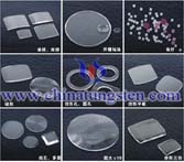 obtain as‐grown optical waveguides of single‐crystalline ZnO on sapphire. The waveguide is made on a very thin sputter‐deposited epitaxial layer of ZnO on sapphire by using the ZnO‐H2‐H2O‐O2 isothermal CVD system. The minimum loss obtained for the TE0 mode propagating perpendicular to the c axis in a ZnO film is 0.7 dB/cm. This chemical‐vapor deposition of ZnO on a thin‐sputtered ZnO film gives a method for the fabrication of strip waveguides on sapphire due to the selective growth of the ZnO films on sputter‐deposited ZnO strips.
Chemically vapour deposited silicon on sapphire (SOS) films 0.25 μm thick were implanted with 28Si+ and recrystallized in solid phase by furnace annealing (FA) and IR rapid thermal annealing (RTA) in our laboratory. An improvement in crystalline quality can be obtained using both annealing procedures. After FA, it is hard to retain the intrinsic high resistivity value (104–105 Ω cm) observed in as-grown SOS films, so the improvement process cannot be put to practical use effectively. However, it is demonstrated that by properly adjusting the implantation and RTA conditions, significant improvements in both film quality and film autodoping can be accomplished. This work describes a modified double solid phase epitaxy process in which the intrinsic high resistivities of the as-grown SOS films are retained. The mechanism of suppression of Al autodoping is discussed.
Tungsten Manufacturer & Supplier: Chinatungsten Online - http://www.chinatungsten.com
Tel.: 86 592 5129696; Fax: 86 592 5129797
Email: sales@chinatungsten.com
Tungsten & Molybdenum Information Bank: http://i.chinatungsten.com
Tungsten News & Tungsten Prices, 3G Version: http://3g.chinatungsten.com
Molybdenum News & Molybdenum Price: http://news.molybdenum.com.cn
Growth And Microstructural Characterization of Catalyst-Free ZnO Nanostructures Grown on Sapphire And GaN by Thermal Evaporation
- Details
- Category: Tungsten & Sapphire Growth Furnace News
- Published on Monday, 16 December 2013 10:13
- Hits: 2449
ZnO nanostructures were grown directly on sapphire substrates and GaN epilayers by thermal evaporation.  Their morphologies and densities were found to be strongly dependent on the synthesis position and the kinds of substrate loaded into the reactor due to the different oxygen densities and the lattice mismatch, respectively. Scanning electron microscopy and transmission electron microscopy studies revealed that ZnO nanorods on sapphire substrates grew in four directions, one sapphire and three sapphire directions. It was found that the in-plane lattice mismatch of inclined ZnO nanorods was remarkably reduced by forming the planar relationship of ZnO//sapphire, compared to that of ZnO//sapphire in the ZnO film. On the other hand, for the GaN epilayers, vertically well-aligned ZnO nanorods were grown after growing an epitaxial ZnO film due to reduced lattice mismatch. Electron energy-loss spectroscopy data showed that Zn-rich stoichiometry was responsible for the formation of ZnO nanostructures.
Results of high-pressure directional growth of GaN on foreign substrates: SiC, sapphire and GaN/sapphire MOCVD templates are presented. The role of nitrogen pressure and supersaturation in the growth process is discussed. The conditions for stable growth of the nitride are determined. The results of the crystallization process are compared with those obtained for directional growth on pressure grown GaN crystals.
Tungsten Manufacturer & Supplier: Chinatungsten Online - http://www.chinatungsten.com
Tel.: 86 592 5129696; Fax: 86 592 5129797
Email: sales@chinatungsten.com
Tungsten & Molybdenum Information Bank: http://i.chinatungsten.com
Tungsten News & Tungsten Prices, 3G Version: http://3g.chinatungsten.com
Molybdenum News & Molybdenum Price: http://news.molybdenum.com.cn
Optical Properties of Clad And Unclad Sapphire Fiber
- Details
- Category: Tungsten & Sapphire Growth Furnace News
- Published on Friday, 13 December 2013 09:54
- Hits: 2501
Single-crystal sapphire fibers have been grown, using the laser heated pedestal technique, with losses as low 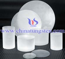 as 0.7 dB/m and with lengths up to 150 cm. We have applied polymer and sol- gel coatings to the fibers and we have evaluated the performance of these coatings as optical cladding. The best coating seems to be teflon AF even though the coatings are reasonably thin and low temperature.
Single crystal layers of formula have been epitaxially grown on formula and sapphire substrates using metallic Zn and Se. A nozzle for the Se flow was placed at about 1 cm in front of the substrate, and this arrangement resulted in much less Se consumption than in the case when the nozzle was further separated from the substrate. The epitaxial conditions were investigated as a function of the source and substrate temperatures. When the substrate temperature and one of the source temperatures were fixed, the growth rate increased with the other source temperature and then saturated. Below the saturation point, the growth rate is proportional to the flow rate and the vapor pressure of each source material. Dependence on substrate temperature of growth rate is shown to be surface‐controlled phenomenon below 770°C and is one of mass transfer controlled phenomena above 770°C. The epitaxial growth on Formula substrates occurred in the substrate temperature range of 650°–880°C with a growth rate ranging from 1 to 30 μm/hr. The resistivity of the as‐grown layer was too high (106 Ω · cm) to be useful for LED application.
Tungsten Manufacturer & Supplier: Chinatungsten Online - http://www.chinatungsten.com
Tel.: 86 592 5129696; Fax: 86 592 5129797
Email: sales@chinatungsten.com
Tungsten & Molybdenum Information Bank: http://i.chinatungsten.com
Tungsten News & Tungsten Prices, 3G Version: http://3g.chinatungsten.com
Molybdenum News & Molybdenum Price: http://news.molybdenum.com.cn
Development of Large Size Sapphire Crystals for Laser Interferometer Gravitational Wave Observatory
- Details
- Category: Tungsten & Sapphire Growth Furnace News
- Published on Friday, 13 December 2013 09:29
- Hits: 2430
Because of its high density and superior quality factor, sapphire crystal, as a candidate material for test 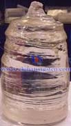 masses, has attracted much attention in gravitation wave communities. The use of sapphire crystal, however, is limited by its size, homogeneity and absorption. An effort has been made at the Shanghai Institute of optics and Fine Mechanics in a collaboration with the Laser Interferometer Gravitational Wave Observatory Laboratory to overcome these difficulties. By using the directional temperature gradient technique, sapphire crystals of 11 cm in diameter and 8 cm in length were grown at the C plane. The results indicate that a homogeneity of <5×10⁻⁷ and an absorption of 35-65 ppm/cm have been achieved at wavelength of 1.06 μm. This paper presents the TGT growth of sapphire crystals, their transmittance spectra, optical homogeneity and absorption. Future applications for gravitational wave experiments are discussed.
The flexure and compressive strengths of sapphire are dependent on crystal orientation and temperature. Most notably, the c -axis compressive strength decreases below the tensile strength at temperatures >400°C and falls to 2% of the room-temperature compressive strength at 800°C. Loss of compressive strength complicates the interpretation of flexure tests. Four-point flexure specimens with no component of c -axis compression increase in strength at temperatures >500°C; however, specimens that have c -axis compression decrease in strength. It has been observed that c -axis compression causes twinning on rhombohedral crystal planes. Intersection of twins on different rhombohedral planes causes fracture that leads to mechanical failure.
Tungsten Manufacturer & Supplier: Chinatungsten Online - http://www.chinatungsten.com
Tel.: 86 592 5129696; Fax: 86 592 5129797
Email: sales@chinatungsten.com
Tungsten & Molybdenum Information Bank: http://i.chinatungsten.com
Tungsten News & Tungsten Prices, 3G Version: http://3g.chinatungsten.com
Molybdenum News & Molybdenum Price: http://news.molybdenum.com.cn
Growth of Bulk GaN Sapphire Single Crystals by The Pressure-Controlled Solution Growth Method
- Details
- Category: Tungsten & Sapphire Growth Furnace News
- Published on Thursday, 12 December 2013 09:47
- Hits: 1191
Gallium nitride was epitaxially grown on sapphire by the vapor phase reaction of Ga-HCl-NH3-Ar system. The  growth rate on sapphire is ∼12 µm/hr, which is higher than that on {0001} sapphire by a factor of ∼1.5. The crystal on sapphire has a lower carrier concentration than that of the same thickness on sapphire by a factor of ∼0.5. The lowest carrier concentration and the highest electron mobility of undoped GaN obtained in this study were 1.6×1019 cm-3 and 78 cm2/V·s, respectively, at 300 K. When heavily doped with Mg, the crystal grown changes markedly in growth morphology. The orientation relationships developed in an undoped or lightly Mg-doped state are GaN//sapphire and GaN//sapphire, and in a heavily doped state GaN//sapphire and GaN//sapphire.
Sapphire single crystal growth of GaN by the pressure-controlled solution growth (PC-SG) method has been carried out using a high-pressure furnace. We have investigated the effect of the supersaturation of nitrogen atoms (the rate of increase of nitrogen pressure) in order to grow large GaN single crystals. It was found that the rate of increase of nitrogen pressure affected the size of a GaN single crystal and its morphology. GaN single crystals with a surface area of about 120 mm2 and/or with good morphology were obtained at a rate less than 49 MPa/h. We have studied the effect of the supersaturation of nitrogen atoms on the crystallinity. The GaN single crystals obtained had the following good crystallinity: (1) the FWHM of the rocking curve was about 120 arcsec without any low-angle grain boundaries, (2) the dislocation density was estimated to be less than 105 cm−2 by TEM observations, and (3) the photoluminescence intensity of the yellowish band became very weak and the PL intensity ratio of the band-edge band to the yellowish band was greatly improved. These results clearly suggest that the rate of increase of the nitrogen pressure in the PC-SG method must be lower to grow large GaN single crystals with good crystallinity.
Tungsten Manufacturer & Supplier: Chinatungsten Online - http://www.chinatungsten.com
Tel.: 86 592 5129696; Fax: 86 592 5129797
Email: sales@chinatungsten.com
Tungsten & Molybdenum Information Bank: http://i.chinatungsten.com
Tungsten News & Tungsten Prices, 3G Version: http://3g.chinatungsten.com
Molybdenum News & Molybdenum Price: http://news.molybdenum.com.cn





 sales@chinatungsten.com