Diameter Dependence of Aligned Growth of Carbon Nanotubes on A-Plane Sapphire Substrates
- Details
- Category: Tungsten & Sapphire Growth Furnace News
- Published on Thursday, 12 December 2013 09:25
- Hits: 2479
Aligned carbon nanotubes have great potential for advanced nanotube transistors and integrated circuits. In this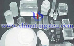 article, we studied the carbon nanotube alignment mechanism using a chemical vapor deposition growth on a-plane sapphire substrates. We synthesized carbon nanotubes of different diameters by controlling the catalyst size and observed that nanotubes of smaller diameters had a higher degree of alignment. In addition, a surprising observation was that misaligned nanotubes had a preferred orientation. Furthermore, we developed a numerical simulation method to calculate interaction energy between a-plane sapphire surface and carbon nanotubes of different diameters. The calculated results were in good agreement with our experimental observations, which confirmed the observed diameter-dependent alignment and the preferred orientation for misaligned nanotubes.
The thermal stability of sapphire was investigated at atmospheric pressure using the in situ gravimetric monitoring (GM) method. The weight change of a sapphire substrate was monitored at various hydrogen partial pressures in carrier gas (Pmath image) at temperatures over 1200 °C. Although the sapphire substrate was stable up to 1450 °C in an inert carrier gas (Pmath image = 0.0 atm), sapphire decomposition started to occur at 1200 °C in H2 carrier gas (Pmath image = 1.0 atm). Moreover the activation energy and order of reaction for sapphire surface decomposition changed at approximately 1300 °C. These results indicate that the rate-limiting reaction for sapphire decomposition shifts near 1300 °C.
Tungsten Manufacturer & Supplier: Chinatungsten Online - http://www.chinatungsten.com
Tel.: 86 592 5129696; Fax: 86 592 5129797
Email: sales@chinatungsten.com
Tungsten & Molybdenum Information Bank: http://i.chinatungsten.com
Tungsten News & Tungsten Prices, 3G Version: http://3g.chinatungsten.com
Molybdenum News & Molybdenum Price: http://news.molybdenum.com.cn
Determination of the Epitaxial Growth of Zinc Oxide Nanowires on sapphire by Grazing Incidence Synchrotron X-Ray Diffraction
- Details
- Category: Tungsten & Sapphire Growth Furnace News
- Published on Wednesday, 11 December 2013 10:10
- Hits: 2556
Hexagonal ZnO nanorods have been selectively synthesized via vapor–solid process without gold catalysis on a  pre-coated ZnO buffer layer. The presence of nanometer-sized pits or hills on the surface of ZnO buffer layer provides nucleation sites to which the zinc vapor is transferred and condensed. Followed by immediate oxidation the ZnO nanorods were grown on the buffer layer. Contrarily, the SEM images hardly show growth of irregular ZnO nanometer-sized products on the bare sapphire substrate. Besides a strong ultra-violet emission at 3.26 eV observed at room temperature, the coupling strength of the radiative transition to LO-phonon polarization field was deduced in use of the Huang–Rhys factor from low temperature photoluminescence spectra to show that single crystalline ZnO nanorods.
It shows that aligned zinc oxide (ZnO) nanowires growth on sapphire substrates is epitaxial and demonstrates the crystallographic relation between the two using grazing incidence synchrotron x-ray diffraction (XRD). The in-plane lattice match between the sapphire and the nanowires was directly probed by using XRD at grazing angles of incidence, where the lattice match between the (0001) plane of the sapphire and the (11-20) plane of the ZnO were observed simultaneously. It will also be shown that gold acts as a catalyst to initiate ZnO nanowire growth, but it does not interfere with the epitaxial mechanism between the nanowires and the sapphire substrate.
Tungsten Manufacturer & Supplier: Chinatungsten Online - http://www.chinatungsten.com
Tel.: 86 592 5129696; Fax: 86 592 5129797
Email: sales@chinatungsten.com
Tungsten & Molybdenum Information Bank: http://i.chinatungsten.com
Tungsten News & Tungsten Prices, 3G Version: http://3g.chinatungsten.com
Molybdenum News & Molybdenum Price: http://news.molybdenum.com.cn
A Century of Sapphire Crystal Growth
- Details
- Category: Tungsten & Sapphire Growth Furnace News
- Published on Wednesday, 11 December 2013 09:55
- Hits: 2417
In Paris around 1890, A. V. L. Verneuil developed a flame fusion process to produce ruby and sapphire crystal. 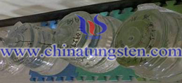 By 1900 there was brisk demand for ruby manufactured by Verneuil's method, which was used with little alteration for 50 years. From 1932-1953, S. K. Popov in the Soviet Union established a capability for manufacturing high quality sapphire crystal by the Verneuil process. In the U.S., under government contract during World War II, Linde Air Products Co. implemented the Verneuil process for making jewel bearings for precision instruments. In the 1960s and 1970s, the Czochralski process was implemented by Linde and its successor, Union Carbide, to make higher quality crystals for ruby lasers. Stimulated by a government contract for structural fibers in 1966, H. LaBelle invented edge-defined film-fed growth (EFG).
The Saphikon company, owned now by Saint-Gobain, evolved from this effort. Stepanov independently developed edge-defined film-fed growth in the Soviet Union. In 1967 F. Schmid and D. Viechnicki at the Army Materials Research Lab grew sapphire by the heat exchanger method (HEM). Schmid later established crystal systems, Inc. around this technology. Rotem Industries, founded in Israel in 1969, perfected the growth of sapphire crystal hemispheres and near-net-shape domes by gradient solidification. In the U.S., growth of near-net-shape sapphire domes was demonstrated by both the EFG and HEM methods in the 1980s but neither method became commercial. Today, domes in the U.S. are made by scooping sapphire boules with diamond-impregnated cutting tools. Commercial markets for sapphire crystal, especially in the semiconductor industry, are healthy and growing at the dawn of the 21st century.
Tungsten Manufacturer & Supplier: Chinatungsten Online - http://www.chinatungsten.com
Tel.: 86 592 5129696; Fax: 86 592 5129797
Email: sales@chinatungsten.com
Tungsten & Molybdenum Information Bank: http://i.chinatungsten.com
Tungsten News & Tungsten Prices, 3G Version: http://3g.chinatungsten.com
Molybdenum News & Molybdenum Price: http://news.molybdenum.com.cn
Advanced Sapphire Furnace Dan Changjing
- Details
- Category: Tungsten & Sapphire Growth Furnace News
- Published on Tuesday, 10 December 2013 09:55
- Hits: 2318
Dan Changjing Advanced Sapphire Furnace (ASF ™) is the production of high quality , the best platform for 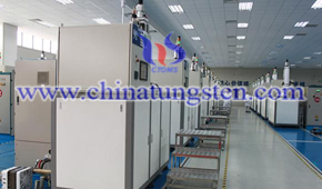 large-size sapphire substrate , sapphire material to meet the highest levels of the market , such as high Brightness LED and other special industrial markets. After 40 years of authentication based on the sapphire crystal growth process and production technology , ASF and low risk , highly automated production environment can operate consistently uniform sapphire ingot material to improve productivity and quality and reduce costs . Furnace production by the ASF sapphire material growth at low heat gradient from low-stress environment , sustainable production of high-quality materials, the most suitable for high-brightness HB LED and other special industrial needs . ASF provides the production of high yields of low-risk method of sapphire , and provide a high return for your investment .
Product main advantages : a rapid growth along the A -axis , a bottom-up manner conducive to the growth of the production of high-quality, low stress sapphire material ; 2 shortest production cycle of less than 18 days ( 100 kg sapphire ingot * ) ; 3 a year. each furnace production capacity exceeds 100,000 TIE;. 4 scalable architecture to protect investment ; 5 based on 40 years after proof sapphire material production ; 6 crucible geometric shape and flexible design process size to meet the requirements of our customers ; 7 no Moving Parts low-cost, low-risk operation and growth of highly automated manufacturing process ; 8 seed simple process.
Tungsten Manufacturer & Supplier: Chinatungsten Online - http://www.chinatungsten.com
Tel.: 86 592 5129696; Fax: 86 592 5129797
Email: sales@chinatungsten.com
Tungsten & Molybdenum Information Bank: http://i.chinatungsten.com
Tungsten News & Tungsten Prices, 3G Version: http://3g.chinatungsten.com
Molybdenum News & Molybdenum Price: http://news.molybdenum.com.cn
Chinese First Super One Hundred kilograms Sapphire Crystal in The Soviet Union Came
- Details
- Category: Tungsten & Sapphire Growth Furnace News
- Published on Tuesday, 10 December 2013 09:51
- Hits: 2423
June 28 morning, in the national scientific and technological progress advanced cities of Zhenjiang born a one 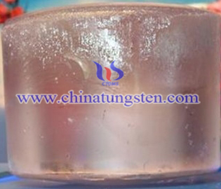 hundred kilograms sapphire crystal , this innovation is the rapid growth of China's LED industry provides a high-quality materials , and means of sapphire crystal growth, substrate manufacturing market long-term dependence on imports passive situation is being broken , to improve the LED industry chain plays a vital role in the history of technological innovation and a milestone. Provincial Science and Technology Department deputy director Wang Qin , vice mayor Feng Shi Chao Zhenjiang City , Zhenjiang Suzhou was party secretary and other relevant leaders , experts and a number of media to witness this moment, it is a body transparent , into a cylindrical shape sapphire crystal , weighing 101.35 kg , is currently produced by human technology largest and heaviest sapphire crystal.
According to on-site technical personnel, over one hundred kilograms Fengyun sapphire crystal with the United States , Switzerland and other foreign experts jointly developed , it is the use of " in-situ growth , in-situ annealing " unique growth process technology for superior quality sapphire single crystal , the crystal growth process solves the inconsistent quality , small size , and many other problems. Successful trial production of the first furnace for future large-scale production and upgrade to a larger size gems possible.
Professor Bai Fengzhou said: Fengyun sapphire crystal far as I can see and understand the size of the country 's largest , heaviest weight sapphire single crystal . Growth process and heat exchange equipment unique in the country , and within a short time large-size sapphire crystal growth hit the ground running , won the first battle . In the process of the domestic large-size sapphire crystal growth in seize the high ground, with the big breakthrough.
Look forward to the next trip, moving steadily, at every step , so that the crystal growth process is stable and reliable equipment operation carefully , the product has a high rate . In particular, firmly grasp the crystal quality, scientific management , advanced technology , and personnel for the fight for more breakthroughs .
In recent years, LED industry is developing rapidly worldwide , and its products are widely used in the field of lighting and blue lasers , especially applied to the liquid crystal display , the market is expanding rapidly , almost 100% of notebook computers, more than 50% of LCD TVs are application . In this huge LED industry chain, sapphire crystal growth, substrate manufacturing at the forefront of LED industry chain is the largest investment , the highest technical barriers, the largest value-added sectors , the manufacturing process each of them requires a high superb production technology and management support , reliance on technology and equipment is very strong, because of this, China's demand for high brightness blue LED epitaxial wafers , etc. are almost entirely dependent on imports . The birth of large-size sapphire crystals , can be said to be a major breakthrough in solving the LED industry chain " bottleneck" .
Tungsten Manufacturer & Supplier: Chinatungsten Online - http://www.chinatungsten.com
Tel.: 86 592 5129696; Fax: 86 592 5129797
Email: sales@chinatungsten.com
Tungsten & Molybdenum Information Bank: http://i.chinatungsten.com
Tungsten News & Tungsten Prices, 3G Version: http://3g.chinatungsten.com
Molybdenum News & Molybdenum Price: http://news.molybdenum.com.cn
Numerical Simulation of Heat And Fluid Flows for Sapphire Single Crystal Growth by The Kyropoulos Method
- Details
- Category: Tungsten & Sapphire Growth Furnace News
- Published on Monday, 09 December 2013 10:41
- Hits: 2636
Numerical computation has been performed to investigate temperature and velocity distributions for different 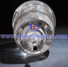 stages of the Kyropoulos sapphire single crystal-growth process. The finite-element method is employed to solve the governing equations with proper boundary conditions. In the power history considered here, a vortex appears in the melt during growth, and its strength decreases as the input power is reduced. Isotherms in the melt are distorted by flow motion. The crystal–melt interface is always convex towards the melt and in early stages the convexity increases as the input power decreases. When the crystal–melt interface is close to the bottom of the crucible, this interface is flat near the apex because of reduction in growth rate near the upper region caused by input heat from the bottom of the crucible. Therefore, convexity of the crystal–melt interface decreases the input power decreases. The crystal shape predicted by the present simulation is similar to that of crystals grown in the industry.
In the present work, 3D features of melt convection during sapphire growth of 100 mm diameter Cz and of 200 mm diameter Ky crystals are studied. The approach accounting for radiative heat exchange with absorption and a specular reflection in the crystal, which we applied in 2D modeling 1, 2 and 3, has been extended to 3D computational domains and coupled to 3D heat transfer in the melt, crystal, and crucible. 3D melt unsteady convection together with crystallization front formation are taken into account within the Direct Numerical Simulation (DNS) approach. Results of 3D modeling are discussed in detail and quantitatively compared to the previously reported data of 2D modeling and experiments 2 and 3. It has been found that the features of unsteady melt convection during the “before seeding”, “seeding”, and “shouldering” growth stages are quite different from each other, which necessitates a flexible control of the radial and vertical temperature gradients in the crucible to provide optimal conditions for stable growth of high quality sapphire crystals.
Tungsten Manufacturer & Supplier: Chinatungsten Online - http://www.chinatungsten.com
Tel.: 86 592 5129696; Fax: 86 592 5129797
Email: sales@chinatungsten.com
Tungsten & Molybdenum Information Bank: http://i.chinatungsten.com
Tungsten News & Tungsten Prices, 3G Version: http://3g.chinatungsten.com
Molybdenum News & Molybdenum Price: http://news.molybdenum.com.cn
Growth And Characterization of Type-II ZnO/ZnTe Core-Shell Nanowire Arrays for Solar Cell Applications
- Details
- Category: Tungsten & Sapphire Growth Furnace News
- Published on Monday, 09 December 2013 10:13
- Hits: 2388
Large area, well-aligned type-II ZnO/ZnTe core-shell nanowire arrays have been fabricated on an a-plane  sapphire substrate. The ZnO nanowires were grown in a furnace by chemical vapor deposition with gold as catalyst and then were coated with a ZnTe shell on the ZnO nanowires surface by a metal-organic chemical deposition chamber. The morphology and size distribution of the ZnO/ZnTe core-shell nanowire arrays were studied by scanning electron microscopy (SEM) and the crystal structure was examined by x-ray diffraction (XRD). Transmission measurement was used to study the optical properties of the core-shell nanowires. The results indicated that the ZnO/ZnTe core-shell nanowire arrays have good crystalline quality. In addition, it was found that the nanowire arrays have good light absorption characteristics and these properties make it suitable for making photovoltaic devices.
ZnTe single crystals were grown by the solution growth method using a Te solvent. The growth has been performed in a vertical Bridgman arrangement. As the seeding material, oriented sapphire substrates with a similar diameter as that of the ZnTe crystals to be grown have been applied. ZnTe single crystals with a diameter of 21 mm could successfully be grown.
Tungsten Manufacturer & Supplier: Chinatungsten Online - http://www.chinatungsten.com
Tel.: 86 592 5129696; Fax: 86 592 5129797
Email: sales@chinatungsten.com
Tungsten & Molybdenum Information Bank: http://i.chinatungsten.com
Tungsten News & Tungsten Prices, 3G Version: http://3g.chinatungsten.com
Molybdenum News & Molybdenum Price: http://news.molybdenum.com.cn
Carbothermal Reduction Growth of ZnO Nanostructures on Sapphire
- Details
- Category: Tungsten & Sapphire Growth Furnace News
- Published on Friday, 06 December 2013 09:59
- Hits: 2397
Zinc oxide (ZnO) nanostructures were grown by the vapour phase transport (VPT) method on a-plane sapphire 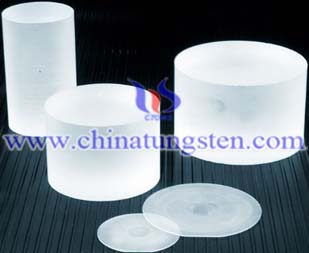 substrates via carbothermal reduction of ZnO powders with various carbon powders. Specifically, graphite powder and activated charcoal powder (of larger total surface area but similar mesh size) were used. ZnO nanostructures can be grown at lower temperatures (∼800 °C) using activated charcoal than those required using graphite powder. Furthermore, the morphologies of ZnO nanostructures obtained using activated charcoal were different to those obtained using graphite. At higher temperatures (∼950 °C), where well-aligned nanorods were obtained using graphite powder, no nanostructures were found using activated charcoal. In contrast to previous results on Si substrates we find that the effects on ZnO nanostructure growth on a-sapphire cannot be explained solely in terms of increased Zn vapour pressure due to the enhancement of the carbothermal reduction reaction rate by the high surface area activated charcoal.
An effective approach is demonstrated for growing large-area, hexagonally patterned, aligned ZnO nanorods. The synthesis uses a catalyst template produced by a self-assembled monolayer of submicron spheres and guided vapor−liquid−solid (VLS) growth on a single crystal alumina substrate. The ZnO nanorods have uniform shape and length, align vertically on the substrate, and are distributed according to the pattern defined by the catalyst template. The nanorods grow along [0001] with side surfaces defined by {21̄1̄0}. This approach opens the possibility of creating patterned one-dimensional nanostructures for applications as sensor arrays, piezoelectric antenna arrays, optoelectronic devices, and interconnects.
Tungsten Manufacturer & Supplier: Chinatungsten Online - http://www.chinatungsten.com
Tel.: 86 592 5129696; Fax: 86 592 5129797
Email: sales@chinatungsten.com
Tungsten & Molybdenum Information Bank: http://i.chinatungsten.com
Tungsten News & Tungsten Prices, 3G Version: http://3g.chinatungsten.com
Molybdenum News & Molybdenum Price: http://news.molybdenum.com.cn
Epitaxial Growth of Large-Area Single-Layer Graphene over Cu/Sapphire by Atmospheric Pressure CVD
- Details
- Category: Tungsten & Sapphire Growth Furnace News
- Published on Friday, 06 December 2013 09:36
- Hits: 2436
We report the atmospheric pressure chemical vapor deposition (CVD) growth of single-layer graphene over a  crystalline Cu film heteroepitaxially deposited on c-plane sapphire. Orientation-controlled, epitaxial single-layer graphene is achieved over the Cu film on sapphire, while a polycrystalline Cu film deposited on a Si wafer gives non-uniform graphene with multi-layer flakes. Moreover, the CVD temperature is found to affect the quality and orientation of graphene grown on the Cu/sapphire substrates. The CVD growth at 1000 °C gives high-quality epitaxial single-layer graphene whose orientation of hexagonal lattice matches with the Cu lattice which is determined by the sapphire’s crystallographic direction. At lower CVD temperature of 900 °C, low-quality graphene with enhanced Raman D band is obtained, and it showed two different orientations of the hexagonal lattice; one matches with the Cu lattice and another rotated by 30°. Carbon isotope-labeling experiment indicates rapid exchange of the surface-adsorbed and gas-supplied carbon atoms at the higher temperature, resulting in the highly crystallized graphene with energetically most stable orientation consistent with the underlying Cu lattice.
Epitaxial monoclinic double tungstate laser crystals were grown with high crystalline quality. Based on these Yb-doped composites, laser operation was demonstrated. Continuous-wave laser emission of a Yb:KYW∕KYW crystal was achieved at 1030nm. The 25‐μm-thin Yb:KYW layer was pumped at wavelengths near 980nm by a Ti:sapphire laser. A maximum output power of 40mW was obtained at room temperature.
Tungsten Manufacturer & Supplier: Chinatungsten Online - http://www.chinatungsten.com
Tel.: 86 592 5129696; Fax: 86 592 5129797
Email: sales@chinatungsten.com
Tungsten & Molybdenum Information Bank: http://i.chinatungsten.com
Tungsten News & Tungsten Prices, 3G Version: http://3g.chinatungsten.com
Molybdenum News & Molybdenum Price: http://news.molybdenum.com.cn
Sasser Sapphire Substrate Shortage
- Details
- Category: Tungsten & Sapphire Growth Furnace News
- Published on Thursday, 05 December 2013 11:05
- Hits: 1218
Upstream chip LED sapphire substrate material due to tight supply, causing prices to rise in the industry has been going on for some time. There is news that two inches sapphire lining  end quote has more than 20 U.S. dollars, the price when compared to the first quarter of 2010, an increase of 50%. Affected by this news will be raising $ 61.5 million, after the expansion of the crystal growth and crystal growth capacity. There were even rumors that Samsung is the opportunity to supply sapphire substrate monopoly against competitors dominated the LED industry to prepare for the future.
Originally an industry level, the elastic material supply and demand, product price changes sentiment index is not worth the fuss. As Sapphire said Li Gang, general manager of Shanghai, currently on the market does appear to be a shortage of supply situation sapphire substrate, a sapphire substrate prices are rising, but have not yet heard of a company which is not on the supply because the sapphire substrate and stop The. Therefore, it can be seen that the current round of sapphire substrates resulting in tight supply, the main reason for rising prices, in fact, the market is in a state of advance warning. If, as some media reports said that nearly 500 sets of MOCVD is installed, there will be a shortage situation indeed, but up to now but formed a production capacity is expected to increase rapidly it seems not too worried. However, further consideration will find a sapphire substrate is expected to make the price rise of 50% in less than six months, which fully reflects the immaturity of young LED industry.
Compare two or three years ago, the solar PV industry, is also emerging industries, greatly concerned the same, the same bright future, under the impetus of Germany, Spain and other state financial subsidies, market demand quickly broke out, but it also causes the whole supply and demand The increase, coupled with the hype man to follow suit, ultimately contradictory to the upstream polysilicon material accumulation stage, gave birth deformities market price: a short period in 2023 pushed up the price of polysilicon materials from around $ 200 to $ 500. In order to grab the express train ride round of ultra-high prices, Chinese companies actually plan out up to 100,000 tons of production capacity of polysilicon material (2006 Chinese annual production capacity is 400 tons), the country was once even sand crucible refining, production of material sources phenomenon. Price collapse affected the healthy development of China is the solar photovoltaic industry.
Now, whether the market demand, or national subsidies, have tilted to the LED industry. But also the emergence of a large number of LED chip factory, these companies also plan an amazing capacity: Sanan Optoelectronics investment, BDO Runda project, Silan private placement in Hong Kong in accordance with national crystallites capital ...... Lighting R & D and Industry Alliance and statistics, in 2010 only on the Chinese mainland is expected to add 140 sets of MOCVD equipment, plus the number of MOCVD manufacturers in Korea and Taiwan of China amplification occurs sapphire substrate, MO gas source as well as other raw material shortages, price rise phenomenon is not surprising. As general manager of Hangzhou Silan Azure Jiang Zhongyong said, the next two years a sapphire substrate shortages are likely to exist, mainly due to the sapphire substrate business less production capacity. It will be driven by the shortage of natural expansion or new business enterprises to join, so that re-balance supply and demand. However, we need to avoid the dramatic ups and downs of price volatility and investment, promote the healthy and orderly trade order and market competition. Otherwise, it would be immature LED supply chain system to form a severe test, and even affect the future development of the whole industry.
Tungsten Manufacturer & Supplier: Chinatungsten Online - http://www.chinatungsten.com
Tel.: 86 592 5129696; Fax: 86 592 5129797
Email: sales@chinatungsten.com
Tungsten & Molybdenum Information Bank: http://i.chinatungsten.com
Tungsten News & Tungsten Prices, 3G Version: http://3g.chinatungsten.com
Molybdenum News & Molybdenum Price: http://news.molybdenum.com.cn




 sales@chinatungsten.com