Sapphire Dan Changjing Tungsten Crucible Furnace
- Details
- Category: Tungsten & Sapphire Growth Furnace News
- Published on Tuesday, 11 March 2014 15:22
- Hits: 2655
First, Sapphire tungsten crucible furnace Dan Changjing About Sapphire Dan Changjing tungsten crucible furnace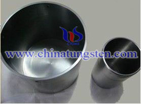
Sapphire Dan Changjing tungsten crucible furnace is one of tungsten products, mainly divided sintering ( applied to the powder metallurgy technique ) , stamping , spinning type . Turning the use of tungsten rod shape ( generally relatively small size ) , forming a variety of welding , the use of pure tungsten plate , tungsten film processing and pure tungsten rod made by the corresponding process . Sapphire Dan Changjing tungsten crucible furnace using an inert gas in a vacuum degrees in 2600 . The melting point of the high boiling point of tungsten , high temperature strength , wear resistant , high thermal conductivity , low coefficient of thermal expansion , good hardenability . Widely used in the tungsten crucible smelting of rare earth , quartz glass, electronic spraying, and other crystal growth sectors .
Tungsten melting point, high boiling point , high temperature strength , anti-friction , corrosion resistance, high thermal conductivity , low coefficient of thermal expansion , good hardenability , thanks to such excellent properties, are widely used in a tungsten crucible smelting of rare earth , quartz glass, electronic spraying , crystal growth and other industries.
Second, Sapphire Dan Changjing tungsten crucible furnace physical and chemical properties
1 Purity : W ≥ 99.95%;
2 , Density : ≥ 18.5g/cm3;
3, The maximum application temperatures : 2400 ℃.
Third, Sapphire Dan Changjing tungsten crucible furnace uses
Since the melting point of tungsten 3410 ℃, and therefore is widely used in the tungsten crucible core container sapphire single crystal growth furnace , quartz glass melting furnace, the rare earth and other industrial furnace, smelting furnace , the use of working temperatures generally above 2000 ℃. Especially for sapphire single crystal growth furnace , the high purity , high density, without internal cracks, precise size , smooth inner and outer walls , and other features of the tungsten crucible for sapphire crystal growth process seed success rate , pulling quality control, from crystal stick pan and life has played a key role.
Tungsten Manufacturer & Supplier: Chinatungsten Online - http://www.chinatungsten.com
Tel.: 86 592 5129696; Fax: 86 592 5129797
Email: sales@chinatungsten.com
Tungsten & Molybdenum Information Bank: http://i.chinatungsten.com
Tungsten News & Tungsten Prices, 3G Version: http://3g.chinatungsten.com
Molybdenum News & Molybdenum Price: http://news.molybdenum.com.cn
What Is A Sapphire?
- Details
- Category: Tungsten & Sapphire Growth Furnace News
- Published on Tuesday, 11 March 2014 13:34
- Hits: 2695
Sapphire (Sapphire) is an alumina (Al2O3) single crystal , the optical penetration with a wide range from the near UV (190nm) to 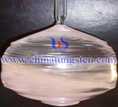 the infrared lens has good optical properties of single crystal alumina . Sapphire crystal has excellent optical properties, mechanical properties and chemical stability , high strength , hardness , corrosion resistance, can work in temperatures close to 2000 ℃ harsh conditions , they have been widely used in military infrared devices , satellite space technology, high-intensity laser window materials . Its unique lattice structure , excellent mechanical properties , good thermal properties make sapphire crystal semiconductor GaN/Al2O3 become practical light-emitting diode (LED), LSI SOI and SOS nanostructured superconducting films and the most ideal substrate material . With the recent LED TV, LED Monitor, LED NB, sustained high growth LED Phone and LED lighting market , driven by strong demand for the production of LED sapphire substrate market expansion.
Since tungsten and molybdenum has a high temperature , low pollution and other characteristics, are widely used to make Sapphire Dan Changjing furnace hot zone components, including tungsten crucible / molybdenum crucible , heating element , tungsten tube, heat shield, support base, the seed rod , the crucible cover. Heating element cage structure using tungsten or tungsten mesh heating element heating element , help provide a uniform and stable temperature field .
Tungsten Manufacturer & Supplier: Chinatungsten Online - http://www.chinatungsten.com
Tel.: 86 592 5129696; Fax: 86 592 5129797
Email: sales@chinatungsten.com
Tungsten & Molybdenum Information Bank: http://i.chinatungsten.com
Tungsten News & Tungsten Prices, 3G Version: http://3g.chinatungsten.com
Molybdenum News & Molybdenum Price: http://news.molybdenum.com.cn
Sided Patterned Sapphire Substrate to Improve Research Performance of Light-Emitting Diodes
- Details
- Category: Tungsten & Sapphire Growth Furnace News
- Published on Monday, 10 March 2014 15:22
- Hits: 2588
There have been many studies regarding increased LED efficiency. The patterned sapphire substrate (PSS) method has been 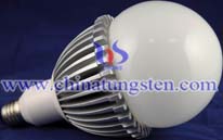 reported to not only improve light extraction efficiency but also increase the internal light efficiency through a low dislocation effect when growing an epitaxial layer growth on the top of the sapphire substrate.3–6 However, these studies are mostly based on lab experiments that are used to show if the efficiency is increased compared to the existing LEDs, which means the quantitative results are somewhat lacking. In order to quantitatively analyze the efficiency improvement from a PSS design, an LED has to pass through many processes. However, there have been studies that quantitatively analyze the improvement of light extraction efficiency through a PSS design in order to develop low cost high intensity LEDs.
This study proposes a new structure that utilizes double-sided patterns on the sapphire substrate in order to increase the light extraction efficiency and heat dissipation efficiency. A Light Tools 7.0 simulation program applying Monte Carlo Method based ray tracing was used to quantitatively analyze the light extraction efficiency of the PSS and to design the pattern. A COMSOL heat transfer simulation was used to analyze the improvement in the heat dissipation efficiency. The designed pattern was applied using a nano imprint lithography (NIL) method to create the pattern on the sapphire substrate used to fabricate and evaluate the actual LED sample.
Tungsten Manufacturer & Supplier: Chinatungsten Online - http://www.chinatungsten.com
Tel.: 86 592 5129696; Fax: 86 592 5129797
Email: sales@chinatungsten.com
Tungsten & Molybdenum Information Bank: http://i.chinatungsten.com
Tungsten News & Tungsten Prices, 3G Version: http://3g.chinatungsten.com
Molybdenum News & Molybdenum Price: http://news.molybdenum.com.cn
Improving Light-Emitting Diode Performance through Sapphire Substrate Double-Side Patterning
- Details
- Category: Tungsten & Sapphire Growth Furnace News
- Published on Monday, 10 March 2014 15:09
- Hits: 2753
Here, we present a new double-side patterned sapphire substrate methodology that improves the efficiency of gallium 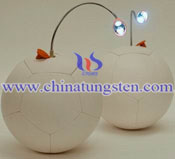 nitride-light emitting diodes (GaN-LEDs). The light extraction efficiency of GaN-based LEDs was analyzed through the use of a ray-tracing simulation. The extraction efficiency was simulated using patterned sapphire substrate LEDs with a variety of shapes, depths, sizes, and spacing. Through the optimal patterning of the various factors, high extraction efficiency was realized and subsequently improved upon. The thermal LED characteristics were analyzed through the use of the COMSOL general heat transfer module. The LEDs patterned on the sapphire substrate were fabricated using nano imprint lithography. We found that the output power of the double-side patterned LED was 52% greater than that of a flat LED. The thermal resistance of the double side patterned LED was 9.5 K/W less than that found for the flat LED.
As the lighting industry continues to advance, the light emitting diode (LED) market share is increasing explosively. The biggest reason for this growth is that LEDs are more energy efficient and have a longer life compared with conventional light sources. The era of full-scale LED applications has arrived as blue and white gallium nitride (GaN) semiconductor based LEDs are commercialized. The LEDs offer the benefits of fast processing speed of a semiconductor and low electricity consumption. As such, they have been accepted into the strategic national product for green growth. The development of the blue GaN LED in the mid-1990s enabled the full-color LED displays that have become a common feature in our daily lives. The high intensity LED market is expanding too fast to measure; efforts to enlarge the chips, improve their luminous efficiency, and the enhancement of their heat dissipation technology support are actively ongoing. However, LEDs have their own problems. The biggest problem is that LED prices are 20 times more expensive than conventional lighting; this is a big burden for their use in households and offices. In order to develop low cost, high intensity LEDs for lighting, more studies regarding luminous efficiency improvement and heat dissipation system development are needed.
Tungsten Manufacturer & Supplier: Chinatungsten Online - http://www.chinatungsten.com
Tel.: 86 592 5129696; Fax: 86 592 5129797
Email: sales@chinatungsten.com
Tungsten & Molybdenum Information Bank: http://i.chinatungsten.com
Tungsten News & Tungsten Prices, 3G Version: http://3g.chinatungsten.com
Molybdenum News & Molybdenum Price: http://news.molybdenum.com.cn
Quasi-Static Characteristics of Microstrip on an Anisotropic Sapphire Substrate
- Details
- Category: Tungsten & Sapphire Growth Furnace News
- Published on Friday, 07 March 2014 10:23
- Hits: 2559
The well-defined and repeatable electrical properties of single crystal sapphire make it an attractive substrate 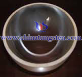 material for microstrip, but its dielectric anisotropy constitutes an important design complication. This paper describes investigations into the quasi-static characteristics of single microstrip lines on sapphire substrates cut with a specified orientation. To account for anisotropy, a new permittivity parameter epsilonreq is introduced, which is a function of the Iinewidth to substrate-height ratio W/h. The variation of epsilonreq with W/h is derived by finite-difference methods. Universal curves for microstrip on correctly orientated sapphire are presented, showing 1) Epsilonreq, 2) The low-frequency limit of effective microstrip permittivity epsilone0, and 3) The characteristic impedance of the line Z0, all as functions of W/h.
A method was developed for depositing silicon films by the pyrolytic decomposition of SiH4 on single crystal sapphire. Electron diffraction and Laue reflection examinations of the films shows single-crystal patterns. The silicon film has a Hall mobility of 135 cm2/volt-second at a hole density of 1017/cm3. Insulated-gate field-effect transistors with a transconductance of 1000 µmho at 5 ma were made with dimensions of 10 µ source-to-drain spacing and an active distance of 120 µ. This value compares favorably with similar units made on bulk silicon and is very encouraging for the possibilities of thin-film silicon devices.
Tungsten Manufacturer & Supplier: Chinatungsten Online - http://www.chinatungsten.com
Tel.: 86 592 5129696; Fax: 86 592 5129797
Email: sales@chinatungsten.com
Tungsten & Molybdenum Information Bank: http://i.chinatungsten.com
Tungsten News & Tungsten Prices, 3G Version: http://3g.chinatungsten.com
Molybdenum News & Molybdenum Price: http://news.molybdenum.com.cn
High Performance GaN-Based LEDs on Patterned Sapphire Substrate with Patterned Composite SiO2/Al2O3 Passivation Layers And TiO2/Al2O3 DBR Backside Reflector
- Details
- Category: Tungsten & Sapphire Growth Furnace News
- Published on Friday, 07 March 2014 10:12
- Hits: 2580
GaN-based light-emitting diodes (LEDs) on patterned sapphire substrate (PSS) with patterned composite  SiO2/Al2O3 passivation layers and TiO2/Al2O3 distributed Bragg reflector (DBR) backside reflector have been proposed and fabricated. Highly passivated Al2O3 layer deposited on indium tin oxide (ITO) layer with excellent uniformity and quality has been achieved with atomic layer deposition (ALD) technology. With a 60 mA current injection, an enhancement of 21.6%, 59.7%, and 63.4% in the light output power (LOP) at 460 nm wavelength was realized for the LED with the patterned composite SiO2/Al2O3 passivation layers, the LED with the patterned composite SiO2/Al2O3 passivation layers and Ag mirror + 3-pair TiO2/SiO2 DBR backside reflector, and the LED with the patterned composite SiO2/Al2O3 passivation layer and Ag mirror + 3-pair ALD-grown TiO2/Al2O3 DBR backside reflector as compared with the conventional LED only with a single SiO2 passivation layer, respectively.
Periodic triangle truncated pyramid arrays are successfully fabricated on the sapphire substrate by a low-cost and high-efficiency laser interference lithography (LIL) system. Through the combination of dry etching and wet etching techniques, the nano-scale patterned sapphire substrate (NPSS) with uniform size is prepared. The period of the patterns is 460 nm as designed to match the wavelength of blue light emitting diode (LED). By improving the stability of the LIL system and optimizing the process parameters, well-defined triangle truncated pyramid arrays can be achieved on the sapphire substrate with diameter of 50.8 mm. The deviation of the bottom width of the triangle truncated pyramid arrays is 6.8%, which is close to the industrial production level of 3%.
Tungsten Manufacturer & Supplier: Chinatungsten Online - http://www.chinatungsten.com
Tel.: 86 592 5129696; Fax: 86 592 5129797
Email: sales@chinatungsten.com
Tungsten & Molybdenum Information Bank: http://i.chinatungsten.com
Tungsten News & Tungsten Prices, 3G Version: http://3g.chinatungsten.com
Molybdenum News & Molybdenum Price: http://news.molybdenum.com.cn
11 PV Industry Company to Profitability
- Details
- Category: Tungsten & Sapphire Growth Furnace News
- Published on Thursday, 06 March 2014 11:42
- Hits: 2591
With the launch of the market for the photovoltaic industry and government policies to support the introduction of intensive photovoltaic industry reversed the first two years of decline . As of yesterday, there are 29 A-share listed companies in the photovoltaic solar energy concepts disclosed the 2013 results of Letters , in which the growth performance of 20 companies , of which 11 achieved a turnaround performance .
Yesterday, New extension to the closing price of 9.40 yuan , intraday stock price was ascribed to 9.68 yuan , but the past two years the share price hit a new high . New extension to the same as this year, photovoltaic solar energy stocks have strengthened. Newspaper Data Center statistics show that a total of 32 cities this year, stocks rose an average of 14.65 percent , far better than the CSI 300 index trend. Among them, the losses of the last Eastern Sunrise , Hengdian East magnetic , Icahn technology, and the results continue to expand pre-hi renewed energy and Kstar , since this year the stock has risen more than 30% .
Photovoltaic solar stocks this year, the trend is so strong reason is due to the dual policy of promoting the PV industry in a good market in the last year out of the previous decline. Warburg Securities latest research report that has experienced the rise of anti- EU and Asia-Pacific emerging markets double , the domestic photovoltaic industry started to recover from the winter , sustained performance improvement . From the entire PV industry chain, the upstream manufacturing enterprises operating rate appeared to improve , gross margin and net margin levels were varying degrees of improvement , profitability continued to improve.
Warburg Securities analyst Ai drizzly new energy that the current PV industry growth continued. First, under the branches and each year the central bank to bank credit policies issued in 2014 , this is the first time for the photovoltaic industry clearly support ; secondly , the National Energy Board recently issued 2014 annual new construction scale photovoltaic notification that requires the construction of photovoltaic power generation this year The total size of the size of annual new record 14 million kilowatts ; third , national Grid has also publicly said the investment will exceed 380 billion this year , photovoltaic priority access . "At present, the photovoltaic industry is subject to market demand in Japan and the U.S. started to usher in a new round of economic cycle ."
Tungsten Manufacturer & Supplier: Chinatungsten Online - http://www.chinatungsten.com
Tel.: 86 592 5129696; Fax: 86 592 5129797
Email: sales@chinatungsten.com
Tungsten & Molybdenum Information Bank: http://i.chinatungsten.com
Tungsten News & Tungsten Prices, 3G Version: http://3g.chinatungsten.com
Molybdenum News & Molybdenum Price: http://news.molybdenum.com.cn
Three Gorges Group Chengde Photovoltaic Power Plant Commissioned
- Details
- Category: Tungsten & Sapphire Growth Furnace News
- Published on Tuesday, 04 March 2014 11:04
- Hits: 2726
Reporter March 3 learned from the Three Gorges Group , which is located in Chengde City, China photovoltaic power plant in northern Hebei grid system as the first large-scale photovoltaic power plant put into operation .
It is reported that the Three Gorges power station by the group's investment in the construction of the Three Gorges New Energy Company , located in Pingquan County , Chengde City . The plant provides about 3.7 million kilowatt-hours per year of green electricity , equivalent to an annual reduction of 12,600 tons of standard coal combustion , conversion to reduce carbon dioxide emissions by 37,600 tons . Three Gorges Group has been put into operation in Hebei Quyang photovoltaic power plant projects there and Shangyi wind power projects.
Pingquan County in Hebei Province in the northeast , the average time between 2800-2900 hours of sunshine , solar energy resources are very rich , and one of the Three Gorges of the Yangtze River into the city by the layout of the photovoltaic industry . Previously, resource development has started cooperation with a number of regional Baoding , Zhangjiakou, Chengde , Tangshan , Xingtai . Expected to " Twelve Five" , the Three Gorges Group's installed capacity built in the Hebei region reached 100 million kilowatts, the scale of investment of about 10 billion yuan , of which wind power, photovoltaic installed capacity of 500,000 kilowatts each .
At present , the Yangtze River Three Gorges Group's new energy sector is mainly borne by the Three Gorges New Energy Company . In 2013 , the Three Gorges New Energy Company in wind power , solar and other new energy fields has made great breakthrough. Xinjiang Hami 200,000 kilowatts of wind power projects in Gansu Guazhou 100,000 kilowatts of photovoltaic projects have grid. Jiangsu Xiangshui 200,000 kilowatts offshore wind farm demonstration project , Inner Mongolia as 400,000 kilowatts of wind power projects approved.
According to statistics, as of the end of 2013 , the Three Gorges New Energy Company's annual installed capacity of 1,403,400 kilowatts new production , the cumulative installed capacity reached 2,963,600 kilowatts . Among them, 2.033 million kilowatts of wind power installed capacity of PV installed capacity of 739,400 kilowatts , small hydropower installed capacity of 191,200 kilowatts . The company's business has covered 30 provinces, autonomous regions and municipalities , members of the unit 100 . With photovoltaic construction slowdown , the Three Gorges New Energy also strengthened procurement and cooperation with Yingli , sun energy.
Tungsten Manufacturer & Supplier: Chinatungsten Online - http://www.chinatungsten.com
Tel.: 86 592 5129696; Fax: 86 592 5129797
Email: sales@chinatungsten.com
Tungsten & Molybdenum Information Bank: http://i.chinatungsten.com
Tungsten News & Tungsten Prices, 3G Version: http://3g.chinatungsten.com
Molybdenum News & Molybdenum Price: http://news.molybdenum.com.cn
Shanxi Accelerate The Healthy Development of The PV Industry
- Details
- Category: Tungsten & Sapphire Growth Furnace News
- Published on Monday, 03 March 2014 14:30
- Hits: 2801
"For PV VAT levy that is the policy of return of 50% , increase with independent intellectual property rights , advanced technology , the development potential of the photovoltaic business credit support , " January 17 , the Shanxi provincial government issued "on accelerate the implementation of views and promote the healthy development of the PV industry , " introduced a number of preferential policies and proposed development goals: " At the end of 2015, the total installed capacity of photovoltaic power generation in Shanxi strive to reach 200 million kilowatts by the end of 2020 , and strive to reach 500 million kilowatts . "
"Opinions" , " actively promote the construction of large-scale photovoltaic power plants and distributed ground stations , focusing on expansion of distributed photovoltaic applications ." Encourage users to follow " self-occupied , the remainder Internet , grid regulation " approach, priority support electricity large , electricity and power law fit high rate of industrial parks , large exhibition venues, supermarkets and other large buildings constructed roof implementation of distributed PV systems. In the use of government funds or energy-saving building schools, hospitals , government agencies , institutions and other office buildings , and actively implement the distributed solar PV . Support the use of photovoltaic power generation in remote areas without electricity and solve the power shortage problem. Encourage urban street lighting , communication base stations , traffic lights, city squares and parks planning and construction of outbuildings emergency photovoltaic power stations .
Late last year on the same slopes Tashan Coal Mine side , to complete the construction of 7 MW solar photovoltaic project in Tashan Industrial Park has become a unique landscape . This is the same coal solar energy , the project started in July 2013 , the building was completed in late 2013 . Reporters learned that the project is 20 megawatts of photovoltaic power generation demonstration project , after the project is completed , there will be the largest photovoltaic power generation base in Shanxi Province .
November 11, 2013 by Luan solar company developed " Luan efficient polycrystalline " batteries official line , the multi- crystalline cell conversion efficiency of 18.44 %. According to reports, " Luan efficient polycrystalline " battery using the back passivation technology to achieve significantly improved cell efficiency , which is Luan solar company through technical innovation and development of a new product , the photovoltaic industry is another major breakthrough. Luan vertically integrated solar energy company industry model , covering all except high-purity polycrystalline silicon photovoltaic industry chain , the products are mainly crystalline silicon ingots and silicon ingots, wafers, cells , solar modules and photovoltaic systems. At present, the annual production capacity reaches 600MW solar Luan integration , performance and quality of the products have reached the international advanced level , high efficiency, high reliability, photovoltaic solar photovoltaic cell technology is the foundation and core technology innovation .
For companies such as Luan solar polysilicon enterprises involved , photovoltaic cells and modules and other projects , "opinions" have proposed specific support measures . In terms of fiscal and taxation policies to support and improve the provincial funds to support the development of mechanisms for the photovoltaic industry , in 2015 , the implementation of photovoltaic VAT levy that is back to 50 % of the policy ; spontaneous personal use of distributed PV electricity tariffs with free collection of various types of government funds and additional ; corporate research and development costs related to compliance with the conditions , in accordance with the tax law in the calculation of taxable income deduction . In terms of financial support , increase with independent intellectual property rights , advanced technology , the development potential of the photovoltaic business credit support , for there is a market , there is order, there are benefits, there are reputable credit PV companies be inclined to increase the credit ; conduct financial products and services innovation , vigorously carry accounts receivable , intellectual property rights , the transfer of ownership , certificates of deposit and other rights as security for loans . Preferential land policies . First, the use of barren hills, slopes , saline land , such as the construction of photovoltaic power generation projects are not utilized , the country in land use planning, plan to be moderately inclined arrangement. Second, the narrow construction land tax, levied on the narrow construction land to the production area, living area and off- road three permanent part . Third, the power plant covers an area of leasing can be paid using a variety of ways . ( Reporter Wang Haibin )
Tungsten Manufacturer & Supplier: Chinatungsten Online - http://www.chinatungsten.com
Tel.: 86 592 5129696; Fax: 86 592 5129797
Email: sales@chinatungsten.com
Tungsten & Molybdenum Information Bank: http://i.chinatungsten.com
Tungsten News & Tungsten Prices, 3G Version: http://3g.chinatungsten.com
Molybdenum News & Molybdenum Price: http://news.molybdenum.com.cn
Wafer Bowing Causes And Mathematical Model
- Details
- Category: Tungsten & Sapphire Growth Furnace News
- Published on Friday, 28 February 2014 11:26
- Hits: 1430
The stress in the films often results from epitaxy in the growth processes and from thermal expansion  coefficient (TEC) mismatch in the postgrowth processes of both metal-organic chemical vapor deposition and hydride vapor phase epitaxy. For example, the stress typically observed is dominated by thermal stress in the post-growth processes, which is usually considered to bring defects or damage to the films, such as, dislocation, buckling, and cracking. Cracks normally extend to the principal tensile stresses within the thin brittle layers and interact with the interfaces of GaN/sapphire. Due to the mismatch of TECs between the GaN film and sapphire, wafer bowing will occur when the GaN film is mechanically constrained by the sapphire after cooling. Thermal stress, wafer bending, and cracking are the main drawbacks that hamper the production of large-area GaN substrates and the application of GaN films. Wafer bowing and stress concentration significantly influence not only the devices’ mechanical performance but also their optical, electrical, and magnetic properties. Therefore, reducing wafer bowing and stress concentration in GaN films is very important. To the best of our knowledge, there are no feasible methods for reducing GaN wafer bowing and few papers on wafer bowing have been published.
When GaN is grown on the sapphire substrate using MOCVD, bowing will happen in epitaxial wafers. There are three major factors for the wafer bowing. One is the temperature difference between the upper and lower interfaces of epitaxial wafers. The lower surface temperature is higher than that of the upper surface, so that the expansion of the lower surface can be larger than that of the upper surface, causing the epitaxial wafers concave. Another is the lattice mismatch between sapphire substrate and epitaxial material, which makes the sapphire suffer from tensile and compressive stress and produces concave or convex bowing. The third is thermal mismatch between epitaxial material and the sapphire substrate, which occurs mainly in the case of a sudden jump or a sudden drop of the outside temperature.
Tungsten Manufacturer & Supplier: Chinatungsten Online - http://www.chinatungsten.com
Tel.: 86 592 5129696; Fax: 86 592 5129797
Email: sales@chinatungsten.com
Tungsten & Molybdenum Information Bank: http://i.chinatungsten.com
Tungsten News & Tungsten Prices, 3G Version: http://3g.chinatungsten.com
Molybdenum News & Molybdenum Price: http://news.molybdenum.com.cn






 sales@chinatungsten.com