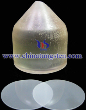
Sapphire Wafer
- Details
- Category: Tungsten & Sapphire Growth Furnace News
- Published on Thursday, 13 February 2014 13:32
Sapphire wafer with complete orientation options including C plane , A plane , R plane and M plane , in  diameter range from 1" to 4" , square substrate is also available as well , size from 10 x 10 mm to 100 x 100 mm . Substrate are produed as per SEMI standards it has good surface finish Ra < 5A and high cleanliness , SWI can offer epi ready grade sapphire wafer for your epitaxial growth . Sapphire wafer are produced by Czochralski method , due to it's high strength, high anti-corrosion high anti-abrasion , low dielectric loss and good electrical insulation , single crystal sapphire wafer plays an increasingly important role as a material for blue LED and high Tc superconductor and microwave applications. Contact us for for further information on price & delivery time .
Thick GaN layers were grown by hydride vapor phase epitaxy (HVPE) with the aim of using these layers as a homoepitaxial substrate to improve device quality of laser diodes or light emitting diodes. HVPE is very useful for thick layer growth since the growth rate can reach from several ten up to one hundred micron per hour. In this experiment, the growth began as selective growth through openings formed in a SiO2 mask. Facets consisting of planes were formed in the early stage and a continuous film developed from the coalescence of these facets on the SiO2 mask. As a result, GaN layers with a dislocation density as low as 6×107 cm-2 were grown on 2-inch-diameter sapphire wafers. These GaN layers were crack-free and had mirror-like surface.
Tungsten Manufacturer & Supplier: Chinatungsten Online - http://www.chinatungsten.com
Tel.: 86 592 5129696; Fax: 86 592 5129797
Email: sales@chinatungsten.com
Tungsten & Molybdenum Information Bank: http://i.chinatungsten.com
Tungsten News & Tungsten Prices, 3G Version: http://3g.chinatungsten.com
Molybdenum News & Molybdenum Price: http://news.molybdenum.com.cn


 sales@chinatungsten.com