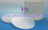
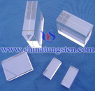
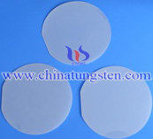
High Strength Bonding of Sapphire
- Details
- Category: Tungsten & Sapphire Growth Furnace News
- Published on Friday, 10 January 2014 11:53
- Hits: 2437
Polycrystalline alumina fillets containing various chemical additives were prepared by tape casting for use in  bonding trials. Oriented sapphire blanks were edge bonded in a furnace with special fixtures to accurately align and apply a load to the components during heat treatment. This approach is consistent with and builds upon the methods used in the previous edge-bonding studies. Flexure strength of the bonded samples, as compared to monolithic sapphire, was used as the performance metric. Additional bonding runs were carried out using the highest performing fillet composition in order to provide a sufficient number of specimens to conduct a Weibull analysis of the failure probability of the bonded material as a function of applied stress.
A high purity alumina composition containing 3 wt.% SiO2, 0.05 wt.% MgO, and
0.05 wt.% Ti, produced the highest strength bonds. This composition yielded an average fracture strength of 255 MPa (37 kpsi), a Weibull modulus of 8.2, and a characteristic strength of 269 MPa (39 kpsi). These results compare favorably to monolithic sapphire specimens which yielded an average fracture strength of 284 MPa (41 kpsi).
Fabrication of GaN Nanowires on Pd-Coated Sapphire Substrates by Magnetron Sputtering Technique
- Details
- Category: Tungsten & Sapphire Growth Furnace News
- Published on Thursday, 09 January 2014 14:58
- Hits: 2193
Large-scale GaN nanowires were successfully synthesized through ammoniating Ga2O3/Pd films sputtered on  the sapphire substrates. X-ray diffraction, scanning electron microscopy, high-resolution transmission electron microscopy, photoluminescence and Raman spectrum were used to characterize the specimens. The results demonstrate that nanowires are single crystal with hexagonal wurtzite structure and have good optical properties. Raman scattering appears broadened and asymmetric compared with those of bulk GaN due to its polycrystalline nature. In addition, the growth mechanism of GaN nanowires is briefly discussed.
Controlled and reproducible growth of GaN nanowires is demonstrated by pulsed low-pressure metalorganic chemical vapor deposition. Using self-assembled Ni nanodots as nucleation sites on sapphire substrates we obtain nanowires of wurtzite-phase GaN with hexagonal cross sections, diameters of about 100 nm, and well-controlled length. The nanowires are highly oriented and perpendicular to the growth surface. The wires have excellent structural and optical properties, as determined by x-ray diffraction, cathodoluminescence, and Raman scattering. The x-ray measurements show that the nanowires are under a complex strain state consistent with a superposition of hydrostatic and biaxial components.
Tungsten Manufacturer & Supplier: Chinatungsten Online - http://www.chinatungsten.com
Tel.: 86 592 5129696; Fax: 86 592 5129797
Email: sales@chinatungsten.com
Tungsten & Molybdenum Information Bank: http://i.chinatungsten.com
Tungsten News & Tungsten Prices, 3G Version: http://3g.chinatungsten.com
Molybdenum News & Molybdenum Price: http://news.molybdenum.com.cn
Microstructural Features And Dislocations on Thermally Etched Sapphire Surfaces
- Details
- Category: Tungsten & Sapphire Growth Furnace News
- Published on Wednesday, 08 January 2014 18:04
- Hits: 2310
Basal, prism and rhombohedral-plane specimens cut and polished from flame-grown sapphire boules  developed fine surface textures during heat-treatment in the range 1700° to 1900°C. Microscopic examinations of such surfaces revealed low-angle grain boundaries, dislocations, and other crystal imperfections. Thermally etched textures apparently were generated by three overlapping processes, namely annealing, etching, and decoration. Thermal etching gave evidence of high-temperature relaxation of residual strain energy introduced at low temperature (analogous to cold work in metals), including that introduced by fracture, microindentation, and cutting and polishing during surface preparation.
Single crystals of Al2O3 (sapphire) were grown from PbO-PbF2 and MoO3-PbF2 fluxes; they varied from flat plates (PbF2-rich melts) to equidimensional crystals (PbO- or MoO3-rich melts). The primary growth planes are basal, first-order rhombohedral, and second-order rhombohedral. The habit change is interpreted on the basis of F- contamination and Pb2+ surface adsorption. Possible ion species in the melts and their relative importance on crystal growth from these systems are discussed.
Tungsten Manufacturer & Supplier: Chinatungsten Online - http://www.chinatungsten.com
Tel.: 86 592 5129696; Fax: 86 592 5129797
Email: sales@chinatungsten.com
Tungsten & Molybdenum Information Bank: http://i.chinatungsten.com
Tungsten News & Tungsten Prices, 3G Version: http://3g.chinatungsten.com
Molybdenum News & Molybdenum Price: http://news.molybdenum.com.cn
ZnO Thin Film Deposition on Sapphire Substrates by Chemical Vapor Deposition
- Details
- Category: Tungsten & Sapphire Growth Furnace News
- Published on Thursday, 09 January 2014 14:44
- Hits: 2196
ZnO thin films with thickness around 200 nm were deposited on a-plane sapphire substrates by Chemical  Vapor Deposition (CVD) method with a mixed ZnO-powder/C-powder solid source. These films were characterized by Atomic Force Microscopy (AFM), Scanning Electron Microscopy (SEM), and photoluminescence (PL) spectroscopy. The correlation between surface structural properties of ZnO thin films and their optical signature measured by temperature dependence of PL is investigated for various growth conditions such as flow rate O2 injection gas and growth temperature. At room temperature, the columbic interaction enhanced absorption edge of 3.305 eV of these films was determined by optical absorption measurements.
Naturally modulated structures,films of In2O3(ZnO)5, were epitaxially grown by rf magnetron sputtering on sapphire substrates. The crystallographic and morphological features of the films were characterized by using x-ray-diffraction and electron-diffraction patterns. The deposition of strongly c axis orientated films of In2Zn5O8 was achieved by epitaxy with a self-buffer layer (SBL). A film of In2Zn5O8 of approximately 10 nm in thickness was initially deposited as the SBL. This initial film was annealedin situ for 10–15 min, after which the bulk of the film of In2Zn5O8 was grown. Finally, well-crystallized In2O3(ZnO)5films were obtained by annealing the resultant film at 800 °C. The electrical properties of the synthesized film are discussed in relation to the mechanism by which the modulated In2O3(ZnO)5 structure is formed.
Tungsten Manufacturer & Supplier: Chinatungsten Online - http://www.chinatungsten.com
Tel.: 86 592 5129696; Fax: 86 592 5129797
Email: sales@chinatungsten.com
Tungsten & Molybdenum Information Bank: http://i.chinatungsten.com
Tungsten News & Tungsten Prices, 3G Version: http://3g.chinatungsten.com
Molybdenum News & Molybdenum Price: http://news.molybdenum.com.cn
Study on Chemical Treatment and High Temperature Nitridation of Sapphire for III-Nitride Heteroepitaxial Growth
- Details
- Category: Tungsten & Sapphire Growth Furnace News
- Published on Wednesday, 08 January 2014 17:47
- Hits: 2295
We have systematically studied the effects of wet chemical etching and high temperature nitridation on the  resulting sapphire surface morphology and chemical transformation. The etching of c-plane sapphire substrates using H2SO4, H3PO4, and a 3:1 H2SO4 :H3PO4 mixture as a function of temperature and etching time was studied and compared with H2 etching at 1100°C and air-annealing at 1400°C. The surface nitridation using NH3 and N2 at 1100°C was studied as a function of NH3 concentration, nitridation time, and surface pretreatment. Atomic force microscopy and x-ray photoelectron spectroscopy were used to study the surface morphology and chemical composition. The detailed surface morphology after chemical etching was a function of the chemical composition and the specific time and temperatures.
The smoothest, pit-free sapphire surface was obtained by etching in pure H2SO4 at 300°C for 30 min. Sulfuric acid etching at higher temperatures or for longer periods generated an insoluble mixture of Al2(SO4)3 and Al2(SO4)3·17H2O crystalline deposits on the surface. Phosphoric acid and the 3:1 H2SO4:H3PO4 mixture etched the sapphire preferentially at defect sites and resulted in pits formation on the surface. The high temperature sapphire nitridation resulted in nitrogen incorporation into the surface. The nitrogen content of nitridation layer depends on NH3 concentration, nitridation time, and surface pretreatment. The nitrogen contents of sapphire treated with H2SO4 and 3:1 H2SO4:H3PO4 are about the same as the as-received sapphire. While the nitrogen content of the air-annealed sapphire is ∼1.6 times higher then the nitrogen content of the as-received sapphire.
Tungsten Manufacturer & Supplier: Chinatungsten Online - http://www.chinatungsten.com
Tel.: 86 592 5129696; Fax: 86 592 5129797
Email: sales@chinatungsten.com
Tungsten & Molybdenum Information Bank: http://i.chinatungsten.com
Tungsten News & Tungsten Prices, 3G Version: http://3g.chinatungsten.com
Molybdenum News & Molybdenum Price: http://news.molybdenum.com.cn
More Articles...
- The Mechanism of Formation of Light-Scattering Centers in Sapphire Crystals Grown in Gas Atmospheres
- Sapphire Crystal Haze Cavity Formation And Annealing Grown by SAPMAC
- Growth of Mg–Al Spinel Microcrystals on a Sapphire Surface Using A Solution-Precipitation Method
- Growth And Process Modeling Studies of Nickel-Catalyzed Metalorganic Chemical Vapor Deposition of GaN Nanowires


 sales@chinatungsten.com