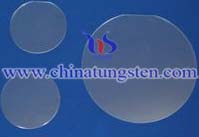
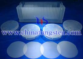
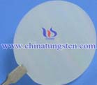
The Sapphire Substrate of Aluminum Nitride Buffer Layer of The Prior Art
- Details
- Category: Tungsten & Sapphire Growth Furnace News
- Published on Thursday, 19 December 2013 09:51
- Hits: 2446
The sapphire substrate of aluminum nitride buffer layer such prior art reference discloses a description by which  the p-type conductivity in the creation of manufacturing a group III nitride semiconductor laser is (AlxGayIn1 - x-yN, including the case of x = 0, Y = 0 and X = Y = 0), by exposure to electron beams. Such a semiconductor laser having formed thereon, in turn, covered with the group III nitride compound semiconductor (AlxGayIn1 - x-yN Sapphire pn heterojunction of the aluminum nitride substrate a buffer layer; including the case x = 0 Next, Y = 0 and x = Y = 0).
In Japanese Unexamined Patent Publication proposed laser diode (closed) Hei-4 - 242985 is a gallium nitride-based compound semiconductor ((the Al x Ga-X) yIn1-YN; 0 ≤ X ≤ 1, 0 ≤ Y ≤ 1), the impurity-doped active layer used.
Tungsten Manufacturer & Supplier: Chinatungsten Online - http://www.chinatungsten.com
Tel.: 86 592 5129696; Fax: 86 592 5129797
Email: sales@chinatungsten.com
Tungsten & Molybdenum Information Bank: http://i.chinatungsten.com
Tungsten News & Tungsten Prices, 3G Version: http://3g.chinatungsten.com
Molybdenum News & Molybdenum Price: http://news.molybdenum.com.cn
Group III Nitride-Based Compound Semiconductor Layer on A Sapphire Substrate
- Details
- Category: Tungsten & Sapphire Growth Furnace News
- Published on Wednesday, 18 December 2013 11:11
- Hits: 2463
A laser diode made of a Group III nitride based compound semiconductor layers comprising a sapphire 
The improved laser diode is made of a gallium nitride base compound semiconductor ((AlxGa1-x)yIn1-yN; 0</=x</=1; 0</=y</=1) with a double heterojunction structure having the active layer held between layers having a greater band gap, the laser diode comprises mirror surfaces formed by cleaving said multi-layered coating and said sapphire substrate in directions parallel to &Lang&0001&Rang& (c axis) of said sapphire substrate. Further, in the improved process, only the intermediate zinc oxide (ZnO) layer is removed by wet etching with a ZnO-selective liquid etchant so as to form gaps between the sapphire substrate and the bottommost sub-layer of said semiconductor laser element layer; and said semiconductor laser element layer is cleaved with the aid of said gaps 20, with the resulting planes of cleavage being used as the mirror surfaces of the laser cavity.
Tungsten Manufacturer & Supplier: Chinatungsten Online - http://www.chinatungsten.com
Tel.: 86 592 5129696; Fax: 86 592 5129797
Email: sales@chinatungsten.com
Tungsten & Molybdenum Information Bank: http://i.chinatungsten.com
Tungsten News & Tungsten Prices, 3G Version: http://3g.chinatungsten.com
Molybdenum News & Molybdenum Price: http://news.molybdenum.com.cn
Synthesis of Single Crystalline GaN Nanoribbons on Sapphire Substrates
- Details
- Category: Tungsten & Sapphire Growth Furnace News
- Published on Tuesday, 17 December 2013 09:59
- Hits: 2339
In previous studies about the synthesis of GaN 1D nanostructures and Ga2O3 only appeared as one of the  components of Ga source. Herein, we have successfully synthesized bulk-quantity GaN nanoribbons on sapphire substrates, from the direct reaction of sputtered Ga2O3 thin films with flowing ammonia. Neither metal catalysts nor templates were used in this process. The detailed characterization of the synthesized ribbon-like 1D nanostructures revealed that they were single crystalline hexagonal wurtzite GaN.
Single crystalline GaN nanoribbons were synthesized through nitriding Ga2O3 thin films deposited on sapphire substrates by radio frequency magnetron sputtering. The component and structure of nanoribbons were investigated by X-ray diffraction (XRD), scanning electron microscopy (SEM), energy-dispersive X-ray (EDX), transmission electron microscopy (TEM) and high-resolution transmission electron microscopy (HRTEM). The flat and smooth ribbon-like nanostructures are high quality single crystalline hexagonal wurtzite GaN. The thickness and width-to-thickness ratio of the grown GaN nanoribbons are in the range of 8–15 nm and ∼5–10, respectively.
Tungsten Manufacturer & Supplier: Chinatungsten Online - http://www.chinatungsten.com
Tel.: 86 592 5129696; Fax: 86 592 5129797
Email: sales@chinatungsten.com
Tungsten & Molybdenum Information Bank: http://i.chinatungsten.com
Tungsten News & Tungsten Prices, 3G Version: http://3g.chinatungsten.com
Molybdenum News & Molybdenum Price: http://news.molybdenum.com.cn
Growth and Characterization of Nonpolar Zn1−xMgxO (0 ≤ x ≤ 0.113) Epitaxial Films: A Comparison of γ-LiAlO2 and Sapphire Substrates
- Details
- Category: Tungsten & Sapphire Growth Furnace News
- Published on Wednesday, 18 December 2013 10:51
- Hits: 2465
γ-LiAlO2 and sapphire substrates have been employed to grow nonpolar Zn1−xMgxO films using metalorganic  chemical vapor deposition. Zn1−xMgxO films with various Mg contents (0 ≤ x ≤ 0.113) are obtained by adjusting the partial pressure of the Mg metalorganic precursor in gas phase. Mg atoms incorporate within the films by means of substituting Zn. No segregated phase such as MgO or metal Mg is observed throughout the Zn1−xMgxO films. Structural characterization of the films indicates that γ-LiAlO2 is a superior substrate to sapphire for the growth of the nonpolar Zn1−xMgxO films.
The epitaxial Zn1−xMgxO films are successfully grown on the γ-LiAlO2 substrates with the epitaxial relationship of ZMO LAO. On the other hand, the Zn1−xMgxO films with both and orientations are obtained on sapphire substrates although Zn1−xMgxO becomes dominant with increasing Mg content. In addition, room-temperature cathodoluminescence spectra of the epitaxial Zn1−xMgxO films show an obvious blue shift of the near-band-edge emission with increasing Mg content, demonstrating bandgap engineering in the epitaxial nonpolar Zn1−xMgxO films on the γ-LiAlO2 substrates.
Tungsten Manufacturer & Supplier: Chinatungsten Online - http://www.chinatungsten.com
Tel.: 86 592 5129696; Fax: 86 592 5129797
Email: sales@chinatungsten.com
Tungsten & Molybdenum Information Bank: http://i.chinatungsten.com
Tungsten News & Tungsten Prices, 3G Version: http://3g.chinatungsten.com
Molybdenum News & Molybdenum Price: http://news.molybdenum.com.cn
Multiple Growth of Profiled Sapphire Crystals
- Details
- Category: Tungsten & Sapphire Growth Furnace News
- Published on Tuesday, 17 December 2013 09:41
- Hits: 2432
Pulling of shaped sapphire crystals using resistance heating implemented by means of heating elements in a  “circular” or a “linear” growth arrangement is described. The growth equipment can be easily disassembled beacause the individual molybdenum dies are connected to a die-holding block with a diffusion Mo-Mo bonding having a reduced strength. Advantages of the individual processes are described and the influence of the die-top temperature upon the quality of pulled crystal shapes is mentioned.
Edge Defined film Fed Growth (EFG) SaphikonTM sapphire crystals have been grown and successfully processed into windows measuring 225 x 325 mm with a thickness of 5.6 mm. More than 40 windows have been completed and assembled into customer hardware and delivered. The polished and coated windows have exhibited average transmission >93% from 1 to 5 mm and wavefront measurements of <0.1 waves rms (@ 0.633 μm) over a 125 mm aperture. Optical measurement data are presented and aspects of the crystal growth and polishing processes are discussed.
Tungsten Manufacturer & Supplier: Chinatungsten Online - http://www.chinatungsten.com
Tel.: 86 592 5129696; Fax: 86 592 5129797
Email: sales@chinatungsten.com
Tungsten & Molybdenum Information Bank: http://i.chinatungsten.com
Tungsten News & Tungsten Prices, 3G Version: http://3g.chinatungsten.com
Molybdenum News & Molybdenum Price: http://news.molybdenum.com.cn
More Articles...
- Optical Properties of Single‐Crystalline ZnO Film Smoothly Chemical‐Vapor Deposited on Intermediately Sputtered Thin ZnO Film on Sapphire
- Growth And Microstructural Characterization of Catalyst-Free ZnO Nanostructures Grown on Sapphire And GaN by Thermal Evaporation
- Optical Properties of Clad And Unclad Sapphire Fiber
- Development of Large Size Sapphire Crystals for Laser Interferometer Gravitational Wave Observatory


 sales@chinatungsten.com