2014 - 2019 Global Alumina Market Increase Nearly 28%- Tungsten Crucible Made Sapphire Market Broaden
- Details
- Category: Tungsten's News
- Published on Tuesday, 23 February 2016 15:48
- Hits: 662
According to international market research report, in 2014-2019, the global high purity alumina market compound annual growth rate will increase nearly 28%. As we known, alumina often referred to as smelter grade alumina (SGA) primarily because it is often used as a raw material for producing aluminum. Alumina mainly be used for aluminum process, only 10% for non-metallurgical alumina market, namely for industrial use.
High purity alumina refers to the minimum purity of 99.99%, and it is high-end products of non-metallurgical alumina market. High purity alumina is a white powder having uniform and easy dispersion particle, stable chemical property, moderate high-temperature shrinkage, good sintering property, high conversion rate, low sodium content and other good property. It is raw material for heat, wear and corrosion products production. Currently, it is used in LED, semiconductor, phosphor, sapphire crystal preparation and other fields.
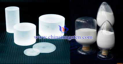
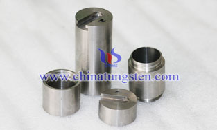
Alumina as raw materials for sapphire single crystal oxide production, with sapphire single crystal applications broaden, the alumina market demand is also growing. Tungsten crucible made sapphire single crystal applications currently on the market are as infrared transparent window materials, microelectronics substrate body, laser matrix, optical components and other purposes.
A study shows sapphire crystal as LED substrate material benefits from the rapid development of LED lighting systems market demand having further expansion, which makes the market demand of sapphire single crystal raw material alumina also having a greater degree of expansion. In 2015 alumina demand growth rate reached 16%. In addition, sapphire crystal applications in the smart phone, making the alumina in this area the growth rate reached 20%. If consider the future use in the mobile phone market, the future demand for alumina and sapphire crystal equivalent to the current needs of the tens times.
| Tungsten Supplier: Chinatungsten Online www.chinatungsten.com | Tel.: 86 592 5129696; Fax: 86 592 5129797;Email:sales@chinatungsten.com |
| Tungsten News & Prices, 3G Version: http://3g.chinatungsten.com | Molybdenum News & Molybdenum Price: http://news.molybdenum.com.cn |
Tungsten Being Applied in Apple Watch 2
- Details
- Category: Tungsten's News
- Published on Monday, 22 February 2016 17:19
- Hits: 695
When Apple announced its much-anticipated Apple Watch back in September 2014, people got very excited about the concept of an Apple-designed smartwatch. Fast forward to today, the Apple Watch has been on sale for quite some time and with 2016 drawing ever closer, people are starting to think about the next-generation Apple Watch, the Apple Watch 2.
Apple is said to be exploring more variations of the Apple Watch, beyond the Sports, Steel and Edition tiers available with the first-gen Apple Watch. It's said that the company is planning to introduce new models that should sit between the most expensive steel Apple Watch (£949) and the cheapest Apple Watch Edition (£8,000).
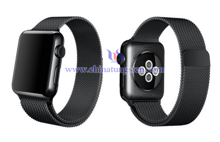
It's looking to attract customers willing to pay between £1,000 and £8,000 for an Apple Watch, however, it's unsure as to how the new tiers will differ from current models.
It's been suggested that the new tier could feature more advanced bands or new materials including tungsten, palladium, titanium or even platinum. Long ago tungsten has been applied in the bracelet of watch which is super tough to prevent surface scratches, also it is rust proven. It’s high density make the watch itself solid but lighter.
| Tungsten Supplier: Chinatungsten Online www.chinatungsten.com | Tel.: 86 592 5129696; Fax: 86 592 5129797;Email:sales@chinatungsten.com |
| Tungsten News & Prices, 3G Version: http://3g.chinatungsten.com | Molybdenum News & Molybdenum Price: http://news.molybdenum.com.cn |
Tungsten Crucible Made Sapphire Wafers - Fingerprint Identification
- Details
- Category: Tungsten's News
- Published on Friday, 19 February 2016 17:19
- Hits: 744

| Tungsten Supplier: Chinatungsten Online www.chinatungsten.com | Tel.: 86 592 5129696; Fax: 86 592 5129797;Email:sales@chinatungsten.com |
| Tungsten News & Prices, 3G Version: http://3g.chinatungsten.com | Molybdenum News & Molybdenum Price: http://news.molybdenum.com.cn |
Ammonium Metatungstate(AMT) Industry China Market Research Report 2016
- Details
- Category: Tungsten's News
- Published on Wednesday, 17 February 2016 15:09
- Hits: 1148
The China Ammonium Metatungstate(AMT) Industry 2016 Market Research Report is a professional and in-depth study on the current state of the Ammonium Metatungstate(AMT) industry.
Russia Plans to Carry Out a Test for Destroying Asteroid by Nuclear Bomb
- Details
- Category: Tungsten's News
- Published on Tuesday, 16 February 2016 14:56
- Hits: 1405
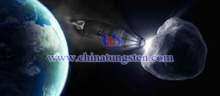

Recently, according to foreign media reports, Russia wants to carry out a nuclear bomb upgrade plan, namely that to emission the nuclear bomb outside of the atmosphere through the intercontinental ballistic missile, in order to destroy asteroids, which would pose a threat to earth.
King of New Materials - Graphene Will Subvert the Future Battlefield, China to Build a Pilot Industry
- Details
- Category: Tungsten's News
- Published on Monday, 15 February 2016 20:16
- Hits: 767
Britain has developed a new technology on rapidly mass production; and Chinese experts successfully developed industrial prospect broad Graphene super battery. The Ministry of industry, national development and Reform Commission and the Ministry of science issued Number Opinions on Accelerating Graphene Industry Innovation and Development. Graphene not only has a broad application prospects in the future, but also will bring disruptive change in the future battlefield.
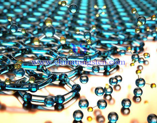
Some scholars said: "nineteenth Century is Iron Age, twentieth Century is Silicon Age, and Twenty-one century is Carbon Age." And Graphene is a representative material of carbon Age. Graphene is stripped out from graphite material, composed of carbon atoms of only one atomic layer, a two-dimensional carbon films with hexagonal honeycomb lattice (benzene). Graphene is a hard material with magic properties of high transmittance, low energy loss. Although graphene has not yet been put into mass production stage, but its excellent performance makes people be full of expectations on the application of future battlefield.
In addition, Graphene is almost zero penetration for gas, liquid and so on. That means coating the ship with Graphene equals to wear a suit of armor "invulnerability". These amazing features also allow Graphene becoming recognized as the king of new materials in just a few decades.
According to opinions, in the future, Graphene will have broad applications on aerospace, weapons and equipment, major infrastructure, and new energy, new energy automotive, energy saving and environmental protection, electronic information and other fields.
| APT Supplier: Chinatungsten Online ammonium-paratungstate.com | Tel.: 86 592 5129696; Fax: 86 592 5129797;Email:sales@chinatungsten.com |
| Tungsten News&Tungsten Prices, 3G Version: http://3g.chinatungsten.com | Molybdenum News & Molybdenum Price: http://news.molybdenum.com.cn |
The United States Worrying China to Sell Semiconductor Equipment at Cabbage Price and Rejected China Takeover of Philps
- Details
- Category: Tungsten's News
- Published on Monday, 15 February 2016 20:12
- Hits: 801
On February 5,New York Times publishedAmerican worrying about Chinese ambition in chip is daily increasing, the article said," China is investing heavily to build the domestic semiconductor industry, the upgrade its military forces and local technology industry's move caused by Washington's attention ". In late January 2016, the U.S. foreign investment committee rejected the Chinese investors take over PHILPS's lighting business at 2 billion 900 million, which is a concrete manifestation of the U.S. government concerns.
So, why the United States obstructed the acquisition? The United States government to stop is not the lighting business itself, but to prevent Chinese investors master the technology of the third generation semiconductor materials—GaN, through the acquisition of Philips’s lighting business. LED of GaN has the smaller appearance, higher power and luminosity than the traditional LED; more critical, the density power of GaN is 10 times of the existing GaAs, which can not only widely be used in communication base station, motor vehicles, electric vehicles, wind power and other civilian areas, but also used in the special fields of phased array radar, and make it became a hotspot and frontier of global semiconductor research.
The reason why U.S government stops Chinese investors’ acquisition of Philips’s lighting business is not just for the considering of technology in military applications and national security, but also for restrains the development of China's semiconductor industry, keep its advantage in technology technical.
In short, China support of the local development of the semiconductor industry in the from of semiconductor, IC design, manufacturing, packaging and testing, semiconductor manufacturing equipment, a full range of support, and strive to achieve a "winner" in the form of the whole industry chain. Once the semiconductor industry captured by China, and output the products at "cabbage price", it can weaken American global supremacy material basis on the one hand; on the other hand, it will make China completely get rid of controlled by others in the field of information technology and the harmful situation of information security, presumably this is what Americans really worries.
| APT Supplier: Chinatungsten Online ammonium-paratungstate.com | Tel.: 86 592 5129696; Fax: 86 592 5129797;Email:sales@chinatungsten.com |
| Tungsten News&Tungsten Prices, 3G Version: http://3g.chinatungsten.com | Molybdenum News & Molybdenum Price: http://news.molybdenum.com.cn |
Tungsten Diselenide is Expected to as Thin Flexible Solar Cells
- Details
- Category: Tungsten's News
- Published on Monday, 15 February 2016 17:42
- Hits: 786
| Tungsten Supplier: Chinatungsten Online www.chinatungsten.com | Tel.: 86 592 5129696; Fax: 86 592 5129797;Email:sales@chinatungsten.com |
| Tungsten News & Prices, 3G Version: http://3g.chinatungsten.com | Molybdenum News & Molybdenum Price: http://news.molybdenum.com.cn |
Tungsten Diselenide has been Developed as New Flexible Solar Cell Materials in Austria
- Details
- Category: Tungsten's News
- Published on Monday, 15 February 2016 17:36
- Hits: 912
| Tungsten Supplier: Chinatungsten Online www.chinatungsten.com | Tel.: 86 592 5129696; Fax: 86 592 5129797;Email:sales@chinatungsten.com |
| Tungsten News & Prices, 3G Version: http://3g.chinatungsten.com | Molybdenum News & Molybdenum Price: http://news.molybdenum.com.cn |
Physical Properties of WTe2 under High Pressure and Strong Magnetic Field II
- Details
- Category: Tungsten's News
- Published on Friday, 05 February 2016 17:15
- Hits: 592
| Tungsten Supplier: Chinatungsten Online www.chinatungsten.com | Tel.: 86 592 5129696; Fax: 86 592 5129797;Email:sales@chinatungsten.com |
| Tungsten News & Prices, 3G Version: http://3g.chinatungsten.com | Molybdenum News & Molybdenum Price: http://news.molybdenum.com.cn |





 sales@chinatungsten.com