Synthesis Of WO3 Nanorods by Thermal Oxidation Technique for NO2 Gas Sensing
- Details
- Category: Tungsten Information
- Published on Wednesday, 08 September 2021 13:12
With the development of industrialization, nitrogen dioxide (NO2) in automobile exhaust and industrial emissions is a serious threat to human health and the ecological environment. 0.1 ppm or even less NO2 will cause significant health effect to human health. Therefore, the highly sensitive NO2 gas sensor has attracted widespread attention. In various gas sensors, metal oxide semiconductor-based sensors are widely applied in industrial, medical and other fields. Due to the presence of several oxidation states of W, tungsten oxide (WO3) is a common sensing material for NO2 semiconductor sensors.
Therefore, WO3 nanorods are synthesized by thermal oxidation technique in atmospheric environment from sputter deposited tungsten film. WO3 nanorods has been synthesized for NO2 gas sensing, the as-prepared gas sensor reveals excellent sensing performance. The synthesis of WO3 nanorods gas sensor device is as below:

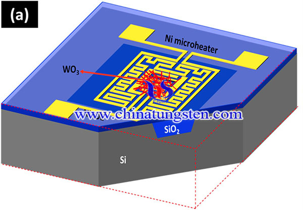
Using radio frequency sputtering technology, a tungsten metal film with a thickness of 100 nm was deposited on a silicon substrate coated with SiO2. The deposited film was oxidized in a horizontal tube furnace at 500°C for 4 hours in an atmospheric environment. Use SEM (model: Zeiss, EVO 18) to observe the morphology of the sample after oxidation, and use XRD (model: Phillips X'pert, Cu Kα X-ray source with a wavelength of 1.54Å) and Raman spectroscopy (model: HORIBA, LabRAM HR Evolution, laser source: 514nm). Use XPS (model: SPECS, Phoibos 100) to study the chemical composition of nanorods. After the WO3 nanorods are grown, the sensor is fabricated using the planar MEMS technology mentioned in our previous publication. The device consists of a miniature heater and the surrounding IDE (Inter Digited Electrode) structure, both of which are placed on a solid thermal insulator. The schematic diagram of the micromechanical gas sensor and its optical image are shown in Figure 1. The size of the device is 1.21mm2, and the minimum feature size is 40μm. The device is manufactured through various micromachining steps such as oxidation, photolithography, anisotropic etching, deposition, chemical mechanical polishing, and lift-off. On this micromechanical platform, it is made by embedding a solid thermal insulator (6μm thick SiO2) in a silicon substrate. The platform reduces heat transmission in local areas, thereby reducing power consumption. When a voltage is applied to the terminals of the micro heater, temperature is generated by Joule heating. For calibration purposes, a DC voltage is applied through the source pad and the current between the two pads is measured at the same time, that is, the resistance is measured at different voltages.

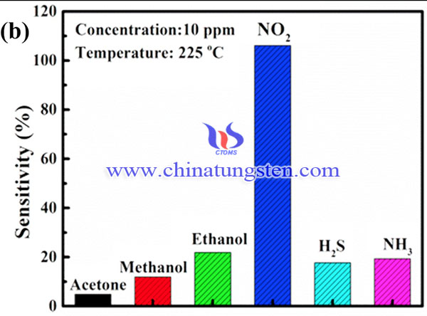
In summary, WO3 nanorods has been synthesized for NO2 gas sensing, the as-prepared gas sensor reveals excellent sensing performance. WO3 nanorods are formed when 100 nm tungsten films oxidized at 500 °C in atmospheric ambient. The result revealed that diameter is ~ 80 nm and length is 400 nm. It showed high response of 116.3% towards 10 ppm of NO2 gas at a moderate optimal operating temperature of 225 °C. At optimal working temperature, the sensor was able to detect small concentration of NO2 gas (2 ppm).
- Tungsten Oxide Manufacturer & Supplier, Chinatungsten Online: www.tungsten-oxide.com
- Tungsten News & Prices of China Tungsten Industry Association: www.ctia.com.cn
- Molybdenum News & Price: news.molybdenum.com.cn
- Tel.: 86 592 5129696; Fax: 86 592 5129797; Email: sales@chinatungsten.com


 sales@chinatungsten.com