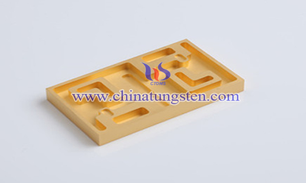
Nanocrystalline Synthetic Tungsten Copper Alloy
- Details
- Category: Tungsten Information
- Published on Saturday, 06 January 2018 22:38
Tungsten copper composite is composed of tungsten and copper, which are not mutually soluble and intermetallic compounds do not form intermetallic monomers. They are generally called tungsten copper pseudo alloys. In large-scale integrated circuits and high-power microwave devices, tungsten copper alloy sheet has broad application prospects as an electronic packaging substrate, connectors, heat sink and microelectronic shell materials.

The traditional method of W-Cu material is a high temperature liquid phase winding and infiltration method. Due to the inherent incompatibility between W and Cu, the density of the alloy prepared by high temperature liquid phase sintering is only about 94-95%. Adding activators such as Ni and Co by activating liquid phase sintering can make the density reach 98 -99%, but the conductivity and thermal conductivity of the alloy have a negative impact.
The method of infiltration is to prepare tungsten skeleton first and then infiltrate Cu into tungsten skeleton pores, though the method is better than that prepared by high temperature liquid sintering. However, the infiltration method of W-Cu material with less than 7wt% copper content is difficult to prepare, and the parts prepared by the method have the advantages of simple shape, coarse and uniform microstructure and poor uniformity of Cu exudation and distribution, affect the material's thermal conductivity and deformation properties.
In recent years, with the development of machining technology toward high accuracy and high complexity, nanocomposite technology for preparing ultrafine / nano W-Cu composite powder can largely alleviate the insolubility of W and Cu, and improve the sintering performance. Some researchers believe that in the preparation process, the use of nanotungsten copper powder, the final preparation of microcrystalline tungsten copper alloy with high density, high uniformity, high thermal conductivity, and can achieve good anti-arc ablation requirements as well as low thermal expansion coefficient of packaging materials for microelectronic devices required tungsten copper material and its preparation method.
Compared with the infiltration method, the densification of nano W-Cu material is more than 98.5%, the microstructure is uniform and fine, the grain size is below 1 m, and the thermal conductivity and arc erosion resistance are improved obviously. The outstanding advantage is that when the tungsten content is high (greater than 80wt%, especially greater than 90wt%), it is difficult to control the penetration of copper and poor material uniformity in the process of preparing tungsten infiltrated copper with high strength. The sintering process is simple, the content of tungsten in the composite material is controllable, components with complex shapes, high-performance electrode materials, electrical contact materials and electronic packaging materials can be manufactured; and large-scale industrial production can be realized.
- Tungsten Alloy Manufacturer & Supplier, Chinatungsten Online: www.tungsten-alloy.com
- Tungsten News & Prices of China Tungsten Industry Association: www.ctia.com.cn
- Molybdenum News & Price: news.molybdenum.com.cn
- Tel.: 86 592 5129696; Fax: 86 592 5129797; Email: sales@chinatungsten.com


 sales@chinatungsten.com