Selective Tungsten Technology Solves Bottleneck to Continued 2D Scaling
- Details
- Category: Tungsten's News
- Published on Thursday, 23 July 2020 20:49
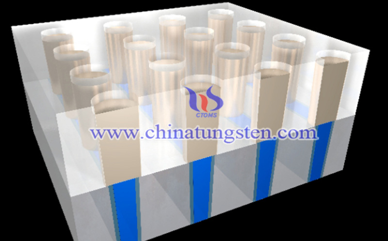
A new selective tungsten process technology has been released by semiconductor equipment manufacturer Applied Materials, Inc. (hereinafter referred to as Applied Materials), which claims to be able to remove a critical bottleneck to continued 2D scaling in foundry-logic nodes.
Applied Materials said that the Applied Endura Volta Selective W CVD system can provide chip manufacturers in a new way to build transistor contacts, which is the first layer of circuitry that links the transistor with other circuits in the chip. This innovative selective deposition technology reduces contact resistance that affects transistor performance and increases power consumption.
Tungsten has been widely used as a gap fill material in middle-of-line (MOL) contacts for its low resistivity and bulk fill characteristics. MOL contacts form the critical electrical link between the transistors and the interconnects. Hence, ensuring low resistivity contacts is crucial for overall device performance.

With continued scaling, however, contact dimensions have decreased to the point at which contact resistance is becoming a bottleneck in realizing optimum device performance. As the cross-sectional area of the contact shrinks, a growing proportion of the volume is occupied by metal liner/barrier and nucleation layers, leaving less volume for the conducting metal fill. Also, multiple resistive interfaces in the plug contribute to higher contact resistance.
Through this technology, node scaling of transistors and their contacts can continue to 5nm, 3nm and below, enabling simultaneous advances in chip power, performance, and area/cost (PPAC).
Although advances in this technology can effectively reduce the size of transistor contact vias, the traditional method of filling the vias with metal will still seriously affect PPAC. Traditionally, transistor contacts are formed in multiple layers. The contact vias are lined with an adhesive layer and a titanium nitride barrier layer, then a nucleation layer is generated by deposition technology, and finally, W is used to fill the remaining space. Tungsten is the first choice for contacting metals due to its low resistivity.
Dan Hutcheson, Chairman and Chief Executive Officer of VLSI Research, a market research organization, said: "The rise of Endura Volta technology to makes it necessary for us to solve some major material engineering challenges to continue 2D scaling. The barrier layer of the liner is like the atherosclerotic plaque of this industry. To obstruct the flow of electrons in the chip, so that the top performance cannot be achieved. Applied Materials' selective tungsten technology is exactly the innovative breakthrough we dream of.
Many leading customers around the world have adopted the new Endura selective tungsten technology system for 2D scaling. This is the latest masterpiece in innovative deposition process technology. The other product portfolios include selective epitaxy, selective deposition, and selective removal. These selective processes allow chip manufacturers to use new methods to make, shape and adjust materials in order to continue to improve in PPAC.
- Tungsten Manufacturer & Supplier, Chinatungsten Online: www.chinatungsten.com
- Tungsten News & Prices of China Tungsten Industry Association: www.ctia.com.cn
- Molybdenum News & Price: news.molybdenum.com.cn
- Tel.: 86 592 5129696; Fax: 86 592 5129797; Email: sales@chinatungsten.com


 sales@chinatungsten.com