Nucleation and Epitaxy of Bilayer Molybdenum Disulfide on Sapphire
- Details
- Category: Tungsten Information
- Published on Thursday, 05 May 2022 22:47
A study conducted mainly by researchers at Nanjing University reports the uniform nucleation (>99%) of bilayer molybdenum disulfide (MoS2) on c-plane sapphire. Two-dimensional transition-metal dichalcogenides (TMDs) are of interest to researchers in the field of electronics. It is believed that the combination of good electrostatic control, smaller bandgap, and higher mobility than single-layer TMDs has the potential to improve the power-delay products of transistors. However, despite the progress made in the growth of single-layer TMDs, multilayer controlled epitaxial growth remains a challenge.

(Credit: Lei Liu / Nature)
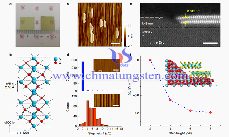
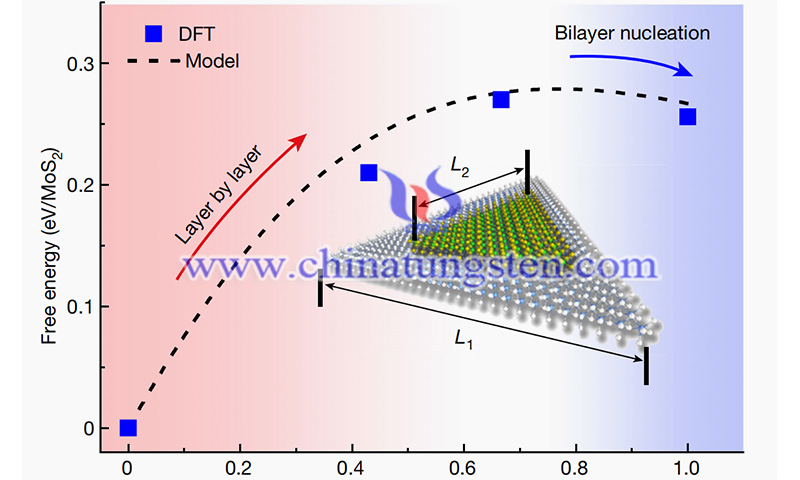
This study designed the height of the atomic terraces on c-plane sapphire so that the edge nucleation mechanism and MoS2 domains coalesce into a continuous, centimeter-scale sheet. The field-effect transistor (FET) devices fabricated based on a double-layer MoS2 channel showed significant improvements in mobility (up to 122.6 cm2 V-1 s-1) and variation compared to the single-layer flake-based FETs. In addition, the short-channel FETs exhibit an on-state current of 1.27 mA μm -1, which exceeds the roadmap target of 2028 for high-performance FETs.
Advanced transistor technology beyond silicon places very stringent requirements on new materials that combine ultimate electrostatic control, sufficient drive current, and large area uniformity. Atomically thin TMDs have the potential to meet these requirements and extend Moore's law beyond the 2 nm node.
However, due to the layer-dependent electronic properties, monolayer TMDs have several fundamental limitations: (1) the inherent mobility (limited by phonon scattering) and density of states are lower than their multilayer counterparts. In reality, the mobility in monolayers is more severely degraded by distant optical phonons and extraneous impurities; (2) the bandgap of about 2 eV leads to large Schottky barrier heights and contact resistances, which ultimately limit the current driving capability of ultrascale FETs. The Fermi-level of the metal-induced gap state further increases the Schottky barrier height of the single-layer TMD.
On the other hand, quantum transport simulations have consistently shown that bilayer TMDs are the most efficient point for balancing performance and power consumption at sub-5 nm nodes. Experimentally, although initial studies of bilayer TMD devices showed better performance, the growth of uniform bilayer molybdenum disulfide films over large areas has proven to be very challenging. Previous attempts using chemical vapor deposition (CVD) could only grow isolated bilayer sheets with limited control over yield, orientation and uniformity. An alternative strategy is layer-by-layer stacking of single layers, but it lacks precise orientation control.

(Credit: Lei Liu / Nature)
Using a kinetically controlled growth process, metal-organic CVD is capable of producing several layers of TMD films and heterostructures by layer-by-layer epitaxy, but the growth rate is several orders of magnitude lower than that of CVD, which limits their practical use. To date, precise layer-controlled TMD epitaxy with large-area uniformity and significant electronic performance advantages has not been demonstrated.
The study titled “Uniform nucleation and epitaxy of bilayer molybdenum disulfide on sapphire” has been published in Nature, Vol 605, 5 May 2022. The study was carried out by Lei Liu, Taotao Li, Liang Ma, Weisheng, Si Gao, Wenjie Sun, Ruikang Dong, Xilu Zou et al.
In summary, this study reports the first scalable, highly oriented, uniform bilayer MoS2 films grown on sapphire substrates by edge nucleation and epitaxy. The study demonstrates more compelling transistor performance than monolayer MoS2, including TMD FET mobility, variability, and record-high ions. This work provides an overall strategy for precise layer control in TMD growth. The researchers predict that bilayer MoS2 is a more competitive channel material that can increase the driving current of transistors while reducing complexity in three-dimensional vertical stacks for better transistor technology.
| Molybdenum Supplier: Chinatungsten Online www.molybdenum.com.cn | Tel.: 86 592 5129696; Fax: 86 592 5129797;Email:sales@chinatungsten.com |
| Tungsten News & Prices, 3G Version: http://3g.chinatungsten.com | Molybdenum News & Molybdenum Price: http://news.molybdenum.com.cn |


 sales@chinatungsten.com