0.7nm Tungsten Selenide (WSe2) Been Developed
- Details
- Category: Tungsten Information
- Published on Monday, 17 June 2019 14:50
0.7nm tungsten diselenide (WSe2) diode has been successfully developed by Dr. Lin’s team from integrated Synchrotron Radiation Research Center of Taiwan Hanyu energy technology company, it’s meaningful of our humans have finally broken the semiconductor 3nm process limit, surpassing Moore's Law and directly entering the sub-nano era (<1 nm). It also reveals that the era of compound semiconductors will eventually replace silicon semiconductors.
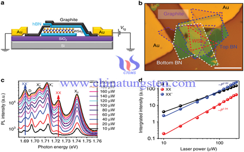
In recent years, despite of improving the basic structure of transistors in integrated circuits, scientists are also actively looking for transistor materials with excellent physical properties, to scaled down to the atomic scale (1 nm), expecting to break through the limits of 3 nm. Dr. Lin’s team developed a tungsten diselenide (WSe2) diode with a single-atomic layer thickness only 0.7nm,it with excellent logic switching characteristics, and his team published the research result in in the journal of Nature Communications.

The main structure of tungsten diselenide (WSe2) consists of a layer of selenium atoms connected to the middle layer of tungsten atoms. The thermal conductivity of tungsten diselenide (WSe2) is about one-hundredth of a million of the best thermal conductivity diamonds, it is the world's lowest thermal conductivity material. The transport electrons responsible for the operation of the tungsten diselenide (WSe2) diode are limited to the single atomic layer, which greatly reduce the interference and increase the operation speed. If it is applied to a digital device in the future, the operation speed is expected to be thousands to ten thousands times higher than the computers we use today. It only consumes very little energy and can meet large energy consumption requirements of chips or machine equipment, if it be used in our phone, then our phone only need to be charged once a month.
Dr. Lin’s team also used a two-dimensional composite of a single layer of tungsten diselenide (WSe2) semiconductor and barium ferrite oxide, for demonstrating the regulation of the electrical properties of two-dimensional materials without metal electrodes, which can turn the current on and off to produce 1 and 0 logic signals. This two-dimensional composite can reduce circuit processs ignificantly and avoid short circuit, leakage or mutual interference.
The birth of two-dimensional single-atom diodes is lighter and more efficient. In addition to the development of electronic components in the post-silicon era beyond Moore's Law, the industry value of component cost/energy/speed optimization is pursued. It can also meet the needs of a large amount of requirements of computing power in future artificial intelligence chips and robot learning.

Tungsten diselenide (WSe2) belongs to two-dimensional material, is a transition metal dichalcogenides (TMDs), tungsten diselenide (WSe2) exhibits excellent semiconductor transmission characteristics in the thickness of the monoatomic layer (about 0.7 nm), which is superior to the conventional silicon semiconductor materials with a thickness of 3 nm. Fully meet the thinner, smaller, and faster needs of next-generation integrated circuits.
Tungsten dioxide (WSe2) diode is not only thinner and lighter, also more efficient. Except it’s industrial value, it also meets the requirements for future artificial intelligence chips and smart equipment, including robotics, computers, and communications.
- Tungsten Manufacturer & Supplier, Chinatungsten Online: www.chinatungsten.com
- Tungsten News & Prices of China Tungsten Industry Association: www.ctia.com.cn
- Molybdenum News & Price: news.molybdenum.com.cn
- Tel.: 86 592 5129696; Fax: 86 592 5129797; Email: sales@chinatungsten.com


 sales@chinatungsten.com