Tungsten Alloy Discs: The "Hardcore" Backbone of the Target Field
- Details
- Category: Tungsten Information
- Published on Friday, 12 September 2025 15:45
- Hits: 12
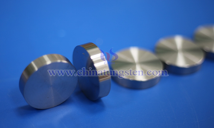
Tungsten (W), renowned as the "industrial tooth" for its high hardness, wear resistance, and chemical stability, plays a pivotal role in materials chemistry and manufacturing. As a refractory metal, tungsten’s atomic structure imparts a high melting point and excellent mechanical strength. When alloyed with elements such as nickel, titanium, or tantalum and formed into discs, its applications in the target field demonstrate outstanding performance.
Chemical Properties of Cut-resistant Tungsten Wire
- Details
- Category: Tungsten Information
- Published on Monday, 03 March 2025 19:44
- Hits: 275
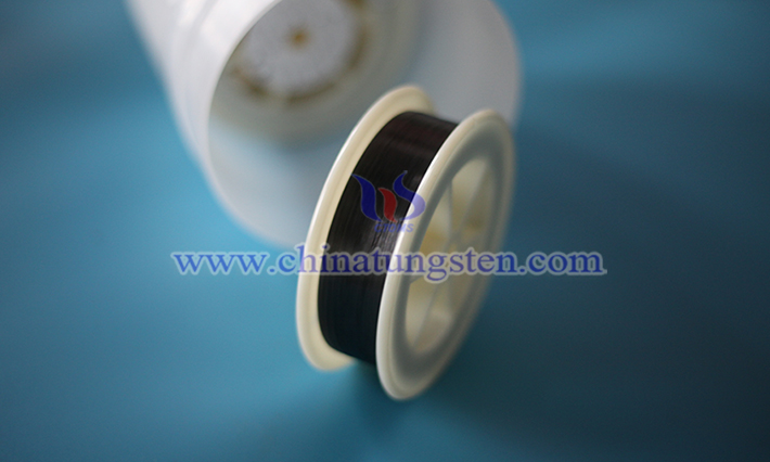
The chemical properties of cut-resistant tungsten wire are primarily based on the chemical characteristics of tungsten metal. Tungsten, a chemical element with the symbol W and atomic number 74, is renowned for its extremely high melting point and chemical stability. Below are the key chemical properties of cut-resistant tungsten wire:
What is Cut-Resistant Tungsten Wire?
- Details
- Category: Tungsten Information
- Published on Monday, 03 March 2025 19:29
- Hits: 237
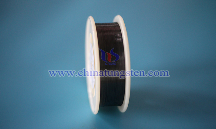
Cut-resistant tungsten wire is a specially treated or modified tungsten-based material. Its core design objective is to enhance resistance to cutting, wear, and high temperatures, making it suitable for scenarios involving high mechanical stress or extreme environments.
Pure Tungsten Electrodes: Key Material in the Welding Industry
- Details
- Category: Tungsten Information
- Published on Wednesday, 26 February 2025 20:24
- Hits: 305
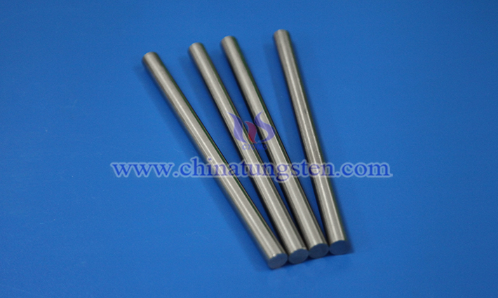
Pure tungsten electrodes, as one of the earliest electrodes used in argon arc welding, have consistently played a significant role in the welding industry. This type of electrode, characterized by its high melting point, high density, corrosion resistance, and excellent electrical and thermal conductivity, has become an indispensable key material under specific welding conditions.
Application of Tungsten and Tungsten Alloys in the Field of Nuclear Fusion Research
- Details
- Category: Tungsten Information
- Published on Friday, 02 August 2024 14:35
- Hits: 855
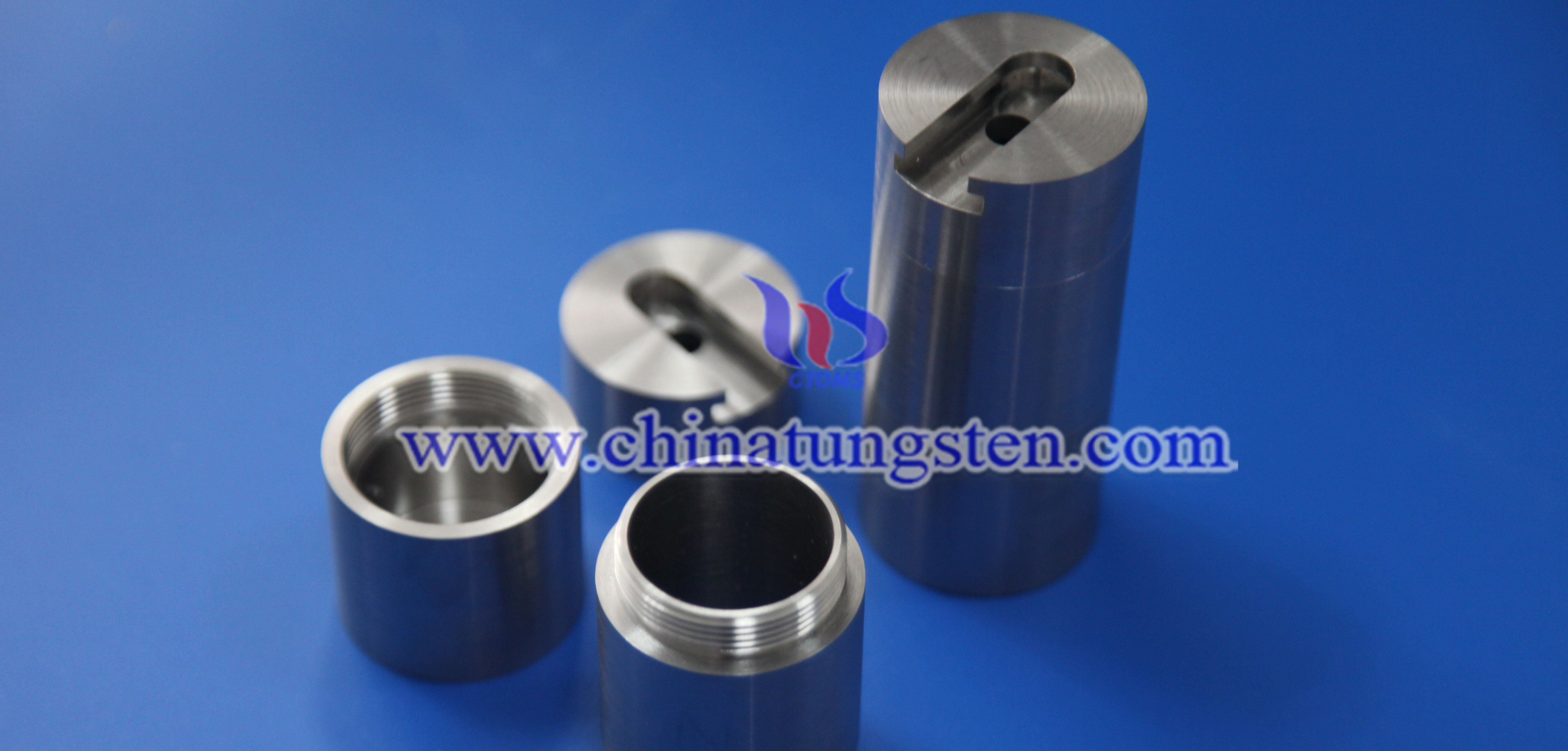
Abstract
Tungsten and its alloys, due to their excellent high-temperature performance, radiation resistance, and mechanical properties, have become ideal candidate materials for key components in nuclear fusion reactors. This paper reviews the progress of research on the application of tungsten and tungsten alloys in the field of nuclear fusion, focusing on their performance in plasma-material interactions, heat load tolerance, and radiation damage. By analyzing current research results and technical challenges, this paper proposes future research directions and development trends, providing a reference for promoting the application of tungsten and tungsten alloys in the field of nuclear fusion.
100 Years of Doped Tungsten WireⅠ- Early Attempts at Metallurgy
- Details
- Category: Tungsten Information
- Published on Wednesday, 13 July 2022 18:47
- Hits: 1443

From a historical perspective, William D. Coolidge's development PM process and tool "for making tungsten ductile" in 1909 marked the beginning of the use of tungsten filaments in the lighting industry. William D. Coolidge's development of the PM process and tools to "make tungsten ductile" in 1909 marked a breakthrough in the use of tungsten filaments in the lighting industry and began the modern industrial era of Powder Metallurgy.
100 Years of Doped Tungsten Wire Ⅳ- Scientific Background of Doped Tungsten Wires and Outlook
- Details
- Category: Tungsten Information
- Published on Wednesday, 13 July 2022 19:43
- Hits: 1378
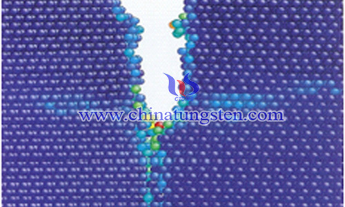
Scientific background of doped tungsten wires
The systematic and purposeful doping of tungsten oxide powders was already patented in 1922. However, the doping of elemental potassium and its role in the formation and stabilization of creep-resistant recrystallization intercalated microstructures was only understood after 1964, when new tools for scanning and transmission electron microscopy and new instruments for surface analysis, especially Auger-Electron-Spectrometry (AES), could be used to perform modern microstructural and chemical analysis of nanometer-sized aggregates. Modern microstructural and chemical analyses were performed.
100 Years of Doped Tungsten Wire Ⅲ - The Invention of Hard Metals
- Details
- Category: Tungsten Information
- Published on Wednesday, 13 July 2022 19:17
- Hits: 1413
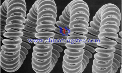
The Invention of Hard Metals
The next important milestone in the chronology of the development of doped tungsten wires is 1923, which marked the year when K. Schröter, chief engineer of the OSRAM research group in Berlin, Germany, made a cemented carbide or hard metal by combining tungsten carbide (WC) and cobalt powder through mixing, pressing and liquid-phase sintering.
100 Years of Doped Tungsten WireⅡ- The Coolidge Process
- Details
- Category: Tungsten Information
- Published on Wednesday, 13 July 2022 19:07
- Hits: 1275
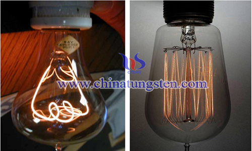
The Coolidge Process
William D. Coolidge (1873-1975), Figure 8, began his career at GE's research laboratory in September 1905. Interestingly, Coolidge's first task was to investigate the cause of the rapid breakage of the filament of the German tantalum lamp when operating under alternating current, most likely due to the limitations of the lamp's cavity technology and the residual gas in the bulb.
Pure Tungsten Pins Is Used for Probes and Cathode Emission
- Details
- Category: Tungsten Information
- Published on Friday, 10 December 2021 10:11
- Hits: 1811
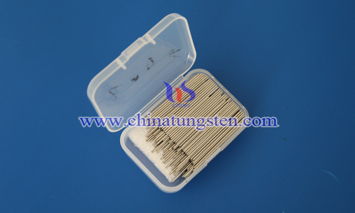
Tungsten pins, also named tungsten needles or tungsten electrodes, are a typical tungsten product with purity of 99.95%. It has a silver-white appearance, a slender structure, a length of 20mm-1000mm, and a diameter of 0.3mm-10mm. Usually, the product is customized.
3D Printed Collimators for Physical Optics Enables Lower Costs
- Details
- Category: Tungsten Information
- Published on Thursday, 09 December 2021 18:50
- Hits: 1783
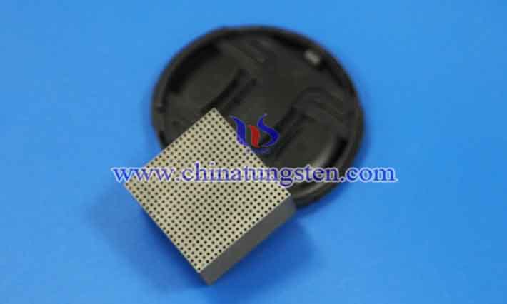
A collimator, a device used to transform the diverging light or other radiation from a point light source into a parallel beam. Special measurements in spectroscopy and in geometric and physical optics require this kind of collimation.
3D Printing Pure Tungsten Parts in the Medical Industry
- Details
- Category: Tungsten Information
- Published on Wednesday, 10 November 2021 11:15
- Hits: 1873
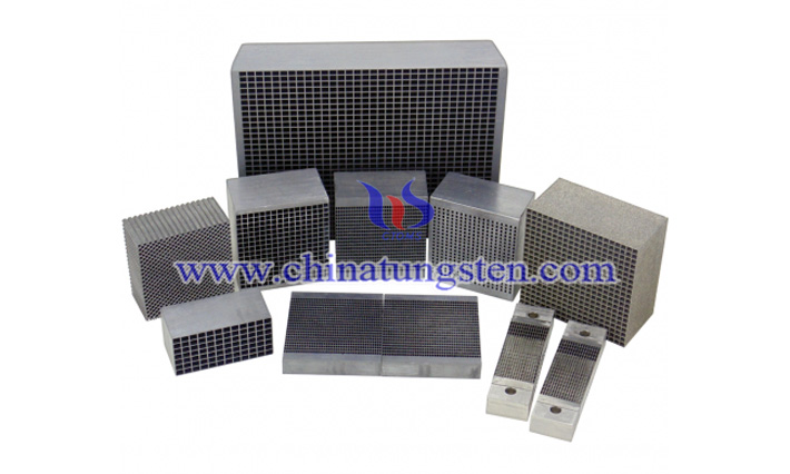
Tungsten, also known as Wolfram, is a rare metal known for its highest melting point of all elements. In addition to excellent temperature resistance, the material also has strong abrasion resistance and chemical resistance. These good properties make it an ideal material for components that operate at extreme temperatures.
What Is the Best Material for X-ray Collimation – Tungsten Metal or Tungsten Alloy?
- Details
- Category: Tungsten Information
- Published on Wednesday, 10 November 2021 09:14
- Hits: 2436
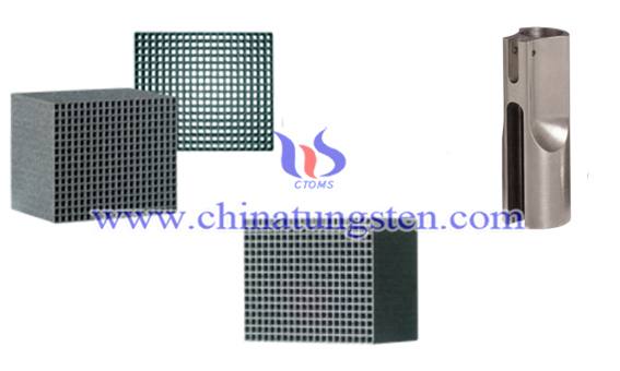
A collimator is a device used to transform the divergent light or other radiation from a point light source into a parallel beam, and also is an absorber device used to limit X-rays, gamma rays, or nuclear particle beams to the size and angular spread required for a specific application. Normally, special measurements in spectroscopy and geometric and physical optics require this kind of light collimation.
Why Use Thorium Tungsten Wires as Ion Source?
- Details
- Category: Tungsten Information
- Published on Thursday, 04 November 2021 09:47
- Hits: 1953
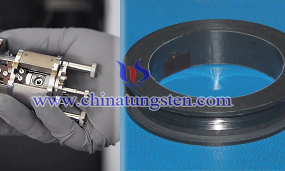
Many analytical and medical devices are using thorium tungsten wires as ion source. Why use thorium tungsten materials? What about tungsten or neodymium tungsten materials?
How is tungsten wire made?
- Details
- Category: Tungsten Information
- Published on Monday, 12 August 2019 09:59
- Hits: 1450
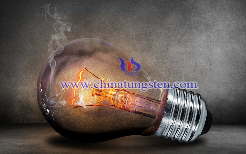
Tungsten wire owns high resistivity and melting point, good strength, and low vapor pressure, which is the best material for making incandescent filaments in all pure metals. However, how is the thin tungsten wire made? As the tungsten is hard, brittle, and difficult to proccess.
Tungsten Disulfide Powder Usage
- Details
- Category: Tungsten Information
- Published on Wednesday, 19 June 2019 21:49
- Hits: 1184
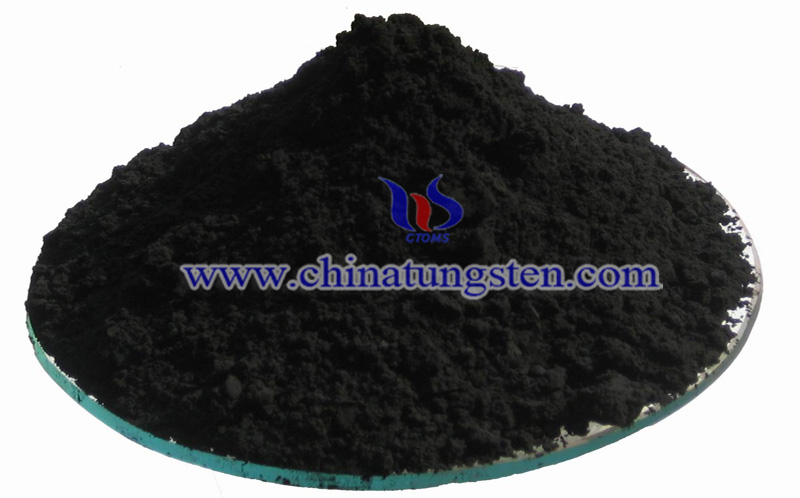
The usage of tungsten disulfide powder is it can be used in high temperature and high-pressure applications. It offers temperature resistance from -450 degree F (-270℃) to 1200 degree F (650℃) in normal atmosphere and from -305 deg F (-188℃) to 2400º F (1316℃) in vacuum.
Tungsten Disulfide Coating
- Details
- Category: Tungsten Information
- Published on Wednesday, 19 June 2019 21:41
- Hits: 1252
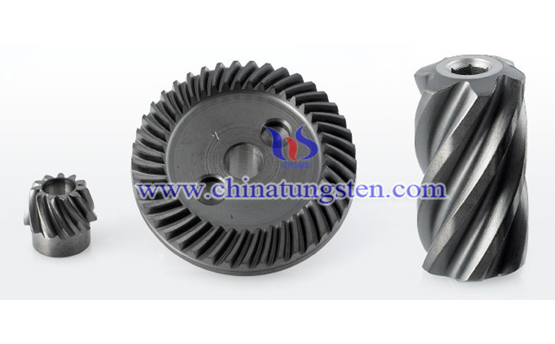
Tungsten disulfide coating is an extremely slick, dry film lubricant coat. WS2 has an extremely low coefficient of friction of 0.03 — lower than that of teflon, graphite, or molybdenum disulfide. The film is remarkably durable compared to many other lubricant materials and can withstand tremendously high loads of over 300,000 psi.
Tungsten Disulfide Applied in Nanotube
- Details
- Category: Tungsten Information
- Published on Wednesday, 19 June 2019 21:30
- Hits: 1257
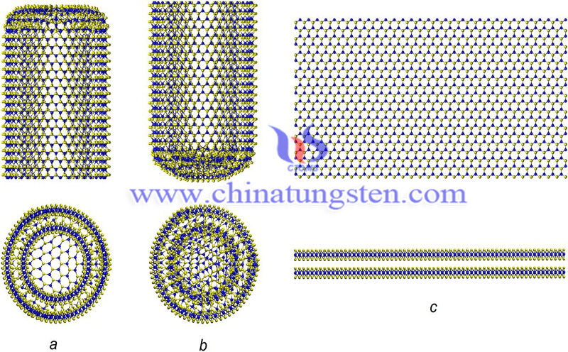
Tungsten disulfide has a layered structure related to MoS2, with W atoms situated in trigonal prismatic coordination sphere. Owing to this layered structure, WS2 forms inorganic nanotube was discovered on an example of WS2 and has been the first material which is able to form it in 1992.
Tungsten Disulfide Property
- Details
- Category: Tungsten Information
- Published on Wednesday, 19 June 2019 21:11
- Hits: 1705
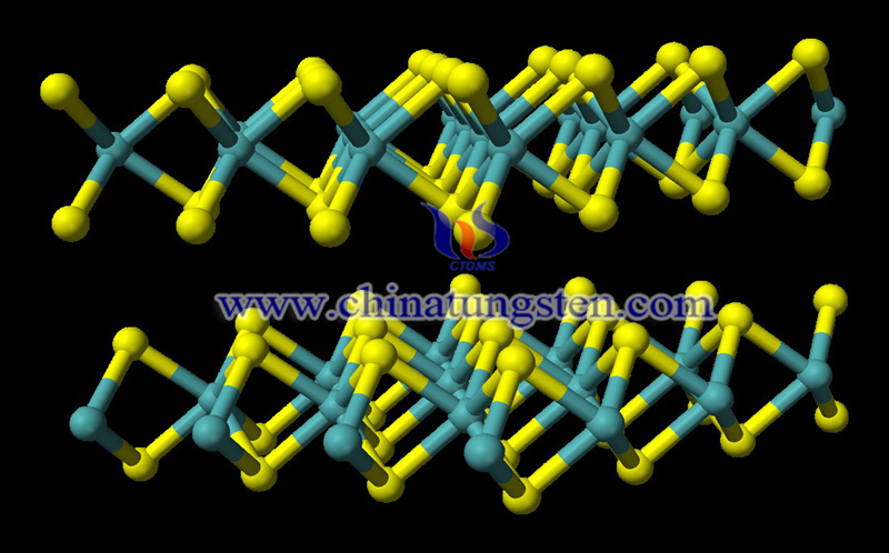
Tungsten disulfide property is diamagnetic, lubricious and easy to be dissociative. It is a compound of tungsten and sulfur, chemical formula is WS2, molecular weight 247.97, the state is black gray powder, appears in the natural world as a tungstenite. The relative density is 7.510. It adopts a layered structure related to MoS2, with W atoms situated in trigonal prismatic coordination sphere.
Spherical Tungsten Carbide Powder Property and Application
- Details
- Category: Tungsten Information
- Published on Tuesday, 18 June 2019 17:51
- Hits: 1087
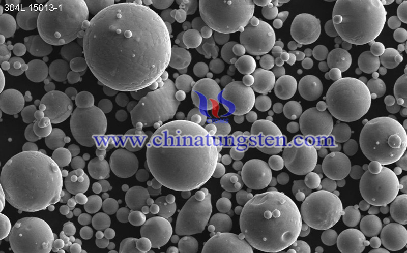
Spherical tungsten carbide powder has the microstructure of fine equiaxed dendrites, its morphology of dense homogeneous spherical WC particles. It maintains a stable chemical property, good fluxibility and hardness, and outstanding wear or abrasion resistance.




 sales@chinatungsten.com