A Novel Model for Band Structure of Monolayer Molybdenum Disulfide
- Details
- Category: Tungsten Information
- Published on Monday, 02 May 2022 11:47
Recently, researchers have proposed an analytical band calculation (ABC) model to study the band structure of monolayer molybdenum disulfide. For two-dimensional (2D) materials, a semiconductor layer is about the thickness of an atomic layer. 2D materials are gaining attention for their potential applications in future transistor manufacturing processes. 2020 International Roadmap for Devices and Systems (IRDS) predicts that by 2028, 2D materials will be the optimal choice for channel material technologies and CMOS 2D device applications.

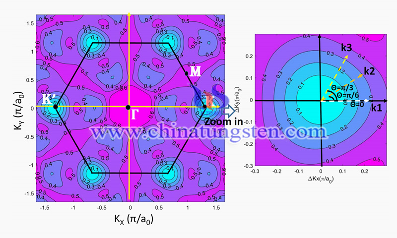
(Credit: Cheng‑Hsien Yang/Journal of Computational Electronics)
2D materials, referring to the thickness of the atomic layers, are layered materials formed by the interaction of atoms in each layer. Van der Waals forces act between the layers. Compared to covalent bonds between molecules, van der Waals forces are extremely small and the layers are easily peeled off, which helps to obtain 2D materials with few or single layers by mechanical techniques. Common 2D materials include graphene, silicene, hexagonal boron nitride, transition metal dichalcogenides (TMD), and black phosphorus (BP) with semiconductor properties.
Monolayer molybdenum disulfide is a tightly packed hexagonal structure. One layer of molybdenum disulfide is in the form of ABA packed with molybdenum and sulfur atoms and is approximately 3.19 Å thick. The cell of molybdenum disulfide resembles two connected triangular pyramidal forms, with the sulfur atoms in the upper and lower layers showing one-sixth of the cell and a molybdenum atom in the center.
Using a new compact band model with simpler computational steps and smaller computation time, the properties of new materials can be analyzed and understood for further applications in TCAD device simulation and SPICE models of 2D devices as indicated in IRDS 2020.

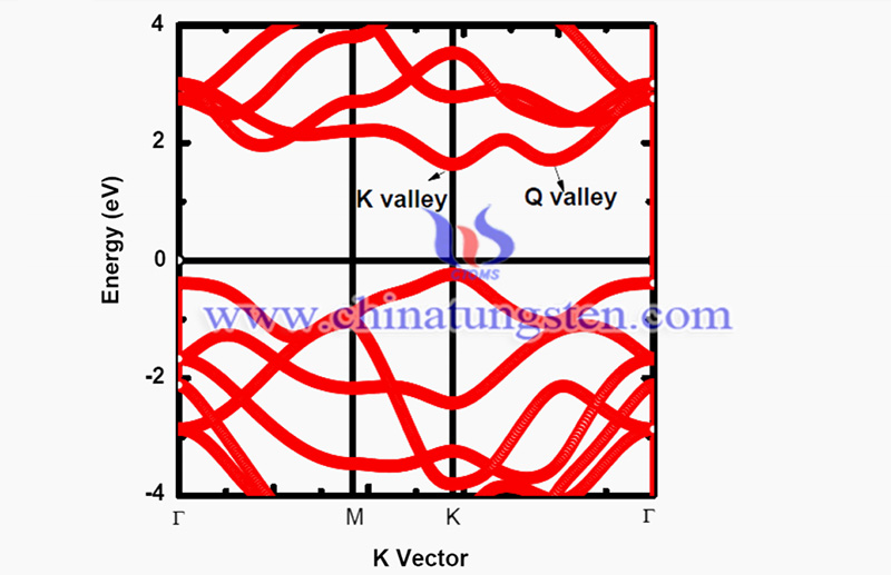
(Credit: Cheng‑Hsien Yang/Journal of Computational Electronics)
The ABC model proposed in this study exhibits triple symmetry in the band structure calculation, which is consistent with the FP model calculation. The ABC model with the Ridley model as the boundary condition can better ft the FP band structure of single-layer MoS2 than the ABC model with the Esseni model as the boundary condition.
The ABC model can be extended to n-fold symmetry to apply to various 2D semiconductor materials. the ABC model is expected to work reasonably well with FP band structure calculations for various 2D semiconductor materials. Finally, the ABC model can be further used to calculate key physical quantities, such as carrier mobility and ballistic current, for various 2D semiconductor materials.
The study titled “Band structure of molybdenum disulfide: from first principle to analytical band model” has been published in the journal of Computational Electronics (2022). The study was carried out by Cheng‑Hsien Yang, Yun‑Fang Chung, Yen‑Shuo Su, Kuan‑Ting Chen, Yi‑Sheng Huang, and Shu‑Tong Chang at National Chung Hsing University.
| Molybdenum Supplier: Chinatungsten Online www.molybdenum.com.cn | Tel.: 86 592 5129696; Fax: 86 592 5129797;Email:sales@chinatungsten.com |
| Tungsten News & Prices, 3G Version: http://3g.chinatungsten.com | Molybdenum News & Molybdenum Price: http://news.molybdenum.com.cn |


 sales@chinatungsten.com