Dimensional Accuracy of Tungsten Cemented Carbide Balls
- Details
- Category: Tungsten Information
- Published on Friday, 12 September 2025 16:47

Tungsten cemented carbide balls (typically made with a metal binder such as tungsten carbide and cobalt) are widely used in high-precision, demanding applications due to their exceptional hardness, wear resistance, corrosion resistance, and stability. Their dimensional accuracy is one of the core criteria for measuring their quality.
Density and Weight Characteristics of Tungsten Carbide Balls
- Details
- Category: Tungsten Information
- Published on Friday, 12 September 2025 16:46
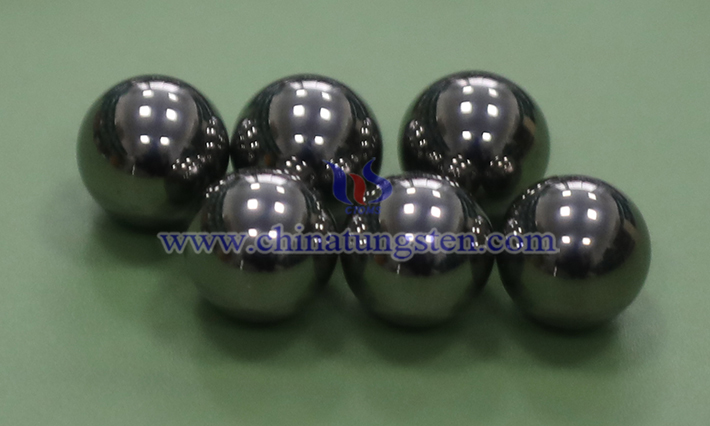
Tungsten carbide balls' core advantages are their high density (typically between 14.5-15.0 g/cm³, with a typical value of 14.9 g/cm³) and excellent weight characteristics. Their density, approximately twice that of steel balls, directly determines their weight distribution, wear resistance, and corrosion resistance. Specific characteristics and their impact are as follows:
Hardness Standards and Test Methods for Tungsten Carbide Balls
- Details
- Category: Tungsten Information
- Published on Friday, 12 September 2025 16:44
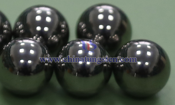
Tungsten carbide balls, composed primarily of tungsten carbide and bonded with cobalt as a binder, are widely used in precision bearings, valves, and molds. Their high hardness and wear resistance are their core properties. Hardness reflects a material's ability to resist local deformation, with typical values ranging from 1500–2000 Vickers hardness (HV). The specific hardness is determined by the alloy grade (such as YG series tungsten-cobalt alloys or YT series titanium-cobalt alloys) and the sintering process. The following briefly describes hardness assessment from the perspectives of standards and test methods.
Chemical Composition of Tungsten Carbide Balls
- Details
- Category: Tungsten Information
- Published on Friday, 12 September 2025 16:43
Tungsten carbide balls are spherical materials made primarily from tungsten carbide powder, a high-hardness refractory metal, combined with a binder and sintered using a powder metallurgy process. Their chemical composition can be summarized as follows:
Main Components and Structure of Tungsten Carbide Balls
- Details
- Category: Tungsten Information
- Published on Friday, 12 September 2025 16:41
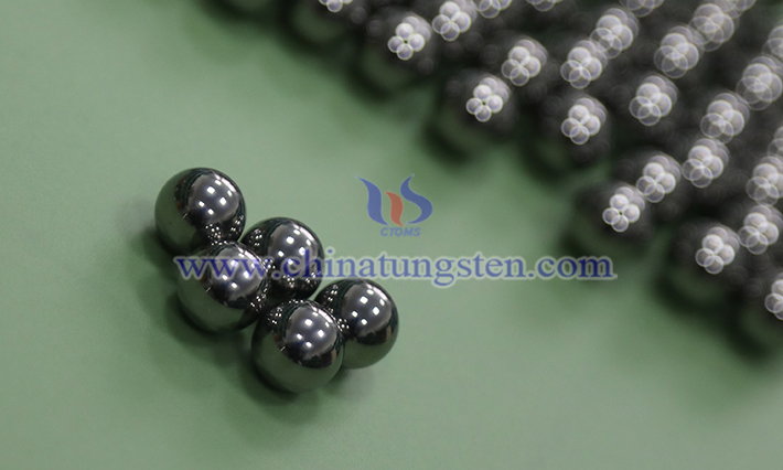
The main components of cemented carbide balls are a highly hard and wear-resistant metal carbide (usually tungsten carbide WC) and a metal binder (usually cobalt Co). The structure can be understood as: hard tungsten carbide particles are encapsulated and bonded by the relatively soft metal cobalt, forming an extremely hard yet moderately tough composite material.
Material Selection for Tungsten Carbide Balls
- Details
- Category: Tungsten Information
- Published on Friday, 12 September 2025 16:40
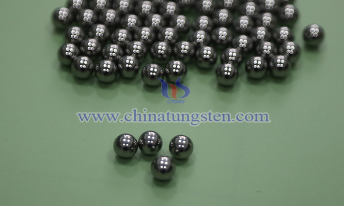
Tungsten carbide balls are manufactured using a powder metallurgy process, combining high-hardness refractory metal carbides as the hard phase and transition metals as the binder phase. Material selection should be centered around core performance requirements. The following is a detailed analysis:
Material Composition of Tungsten Cemented Carbide Balls
- Details
- Category: Tungsten Information
- Published on Friday, 12 September 2025 16:38
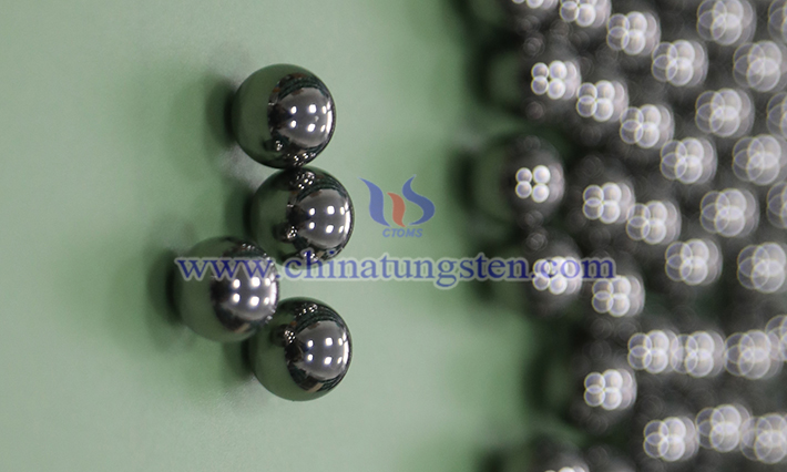
As the name suggests, tungsten cemented carbide balls are primarily made of cemented carbide. Cemented carbide is not a single metal, but rather a composite material composed of high-hardness, high-melting-point metal carbides and a metal binder, manufactured through a powder metallurgy process. Its core composition can be summarized as a "two-phase structure":
Materials for Tungsten Cemented Carbide Balls
- Details
- Category: Tungsten Information
- Published on Friday, 12 September 2025 16:37
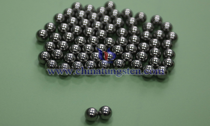
I. Main Materials for Tungsten Cemented Carbide Balls 1. Tungsten Carbide (WC):
This is the primary component of tungsten cemented carbide balls. It possesses extremely high hardness and wear resistance, and serves as the core material providing the ball's strength.
Surface Quality Inspection Methods for Tungsten Cemented Carbide Balls
- Details
- Category: Tungsten Information
- Published on Friday, 12 September 2025 16:35
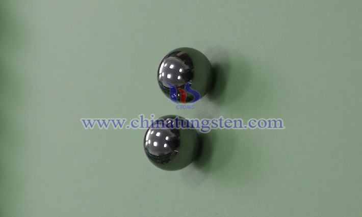
Due to their high hardness, wear resistance, and excellent mechanical properties, tungsten cemented carbide balls are widely used in precision bearings, valve seals, and measuring instruments. Their surface quality directly impacts service life, sealing performance, and operating accuracy, making surface quality inspection a critical step in production and application. Surface quality inspection primarily focuses on defects (such as cracks, pits, scratches, and pores), roughness, uniformity, and residual stress. The following introduces several commonly used inspection methods, combining traditional techniques with modern nondestructive testing methods to address various precision requirements and production scenarios.
Tungsten Carbide Balls Quality Control
- Details
- Category: Tungsten Information
- Published on Friday, 12 September 2025 16:28
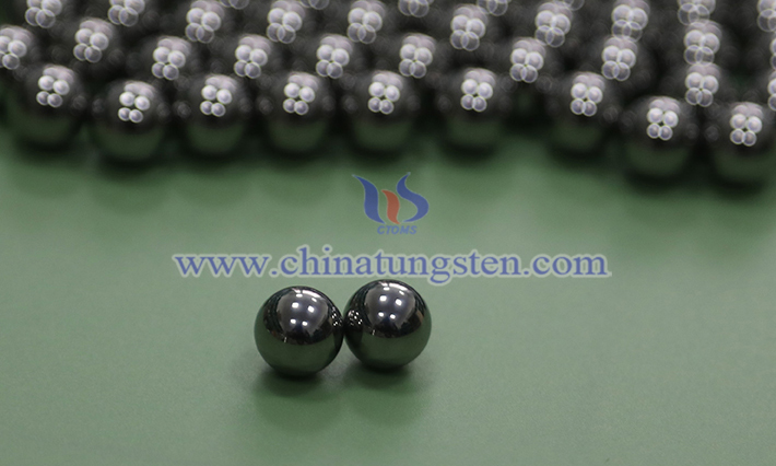
Quality control of tungsten carbide balls is critical to ensuring their performance meets application requirements. This requires comprehensive management from raw materials and production processes to finished product testing, combining advanced testing methods with rigorous process monitoring to ensure stable product performance.


 sales@chinatungsten.com