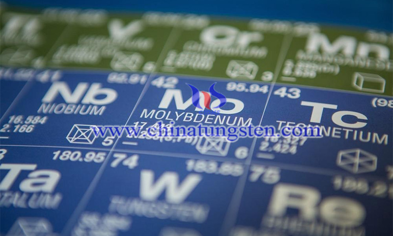
Creating A 2D Semiconductor from Molybdenum Disulfide
- Details
- Category: Tungsten's News
- Published on Thursday, 25 November 2021 22:35
The field of semiconductor research is constantly exploring materials with enhanced properties, and Andras Kis from École Polytechnique Fédérale de Lausanne, Lausanne, Switzerland writes in Nature about how his team created a 2D semiconductor based on a single layer of inorganic molybdenum disulfide (MoS2).
Moore's Law states that the number of transistors on a semiconductor will double every two years. In pursuit of this goal, the materials used in semiconductors continue to get thinner. How thin material can be is a key question in semiconductor design. Solving this dilemma will inform the future of the industry, providing innovative technologies that will help the industry take a big step forward and address the limitations of semiconductor design.
Andras Kis' group at EPFL in Switzerland began exploring the fabrication of two-dimensional molybdenum disulfide transistors. These films are stripped from massive crystals. The microscopy supplies market sells molybdenite, a mineral composed of MoS2 that is similar in appearance to graphite.

Fabricating transistors using this material was challenging, and one of the early challenges was the need to find a suitable contact material. Progress toward solving this difficulty was made by the end of 2009, when transistors were routinely produced using five to six layers of thick molybdenum disulfide. These early transistors showed current modulation of six orders of magnitude. However, single-layer transistors still faced problems with noise and resistance.
This was done by depositing the insulating material layer by layer using an atomic layer deposition system, developed by Aleksandra Radenovic. To further explore protection against air and moisture and to shield the two-dimensional material from impurities, the team investigated the application of hafnium oxide. This worked better than the research team had expected.
The team's first generation single layer transistor device shows enhanced electrical characteristics and performance. Current and resistance show significant improvements, with on/off current ratios in excess of 1x10⁸ observed.
Meanwhile, research groups at the University of California, Berkeley, Trinity College Dublin, and Columbia University have been studying the properties and manufacturing methods of molybdenum disulfide. The results of the research conducted by these groups have provided some significant advances in the field.
First, a team of researchers at Berkeley and Columbia University demonstrated that monolayers of molybdenum sulfide exhibit photoluminescence due to their band gap. The team at Trinity College Dublin developed a liquid-phase exfoliation process to produce MoS2, as well as other two-dimensional monolayers, on a large scale. These findings, along with the fabrication of two-dimensional monolayer molybdenum disulfide transistors, pave the way for expansion in this field.
Two-dimensional transistors are revolutionary to the semiconductor industry, and these atomically thin devices have the potential to enable the continued expansion of transistors across a wide range of devices. However, much of the research on 2D semiconductor to date has been limited to proof-of-concept, and the field needs significant work to evaluate these devices and achieve their commercial viability in the electronics industry.
As the demand for atomic-scale materials grows, research into ultra-thin devices is accelerating, and Kis and his team's groundbreaking research offers new opportunities for physicists, chemists and engineers working in the semiconductor industry to realize the true limits of semiconductor technology.
| Molybdenum Supplier: Chinatungsten Online www.molybdenum.com.cn | Tel.: 86 592 5129696; Fax: 86 592 5129797;Email:sales@chinatungsten.com |
| Tungsten News & Prices, 3G Version: http://3g.chinatungsten.com | Molybdenum News & Molybdenum Price: http://news.molybdenum.com.cn |


 sales@chinatungsten.com