WSe2 Monolayer Integrated onto SiN Waveguide, A Crucial Step in Quantum Photonics
- Details
- Category: Tungsten's News
- Published on Wednesday, 23 October 2019 14:05
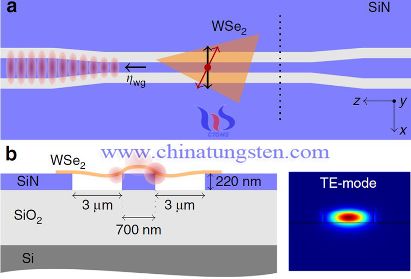
Researchers integrate the tungsten disilicide (WSe2) monolayer onto a silicon nitride (SiN) photonic chip to couple the quantum emitter to the waveguide. According to MEMS Consulting, researchers from the Imec research center, Ghent University and MIT announced that they have integrated single-photon emitters in 2D layered materials with a silicon nitride photonic chip. Even for moderate quantum yields, dielectric cavities could be designed such that the single-photon extraction into the guided mode can reach unity. The results published in Nature Communications, provide a crucial step in fundamental quantum photonics and 2D materials.

Photonic integrated circuits (PICs) enable the miniaturization of complex quantum photonic circuits with large numbers of photonic devices connected with optimized insertion losses and phase stability. Single-photon emitters (SPEs) are the core components of such quantum integrated circuits, and various material systems have been studied to fabricate such on-chip SPEs. 2D-SPE owns some unique properties that make it ideal for integration with PIC. First, they can be easily connected to the PIC to form complex heterostructures by stacking. Second, because of their thin thickness and no total internal reflection, very high light extraction efficiency can be achieved without any additional processing. Third, it becomes easier to grow 2D materials that produce wafer-level high uniformity.
![]()
In PIC, photons are routed in a single spatial mode along a low-loss single-mode waveguide consisting of high-refractive cores and high-refractive clad materials. PIC allows for the integration of multiple functions on a single chip, including photonic cavities that enhance photo-substance interaction, filters that block or select specific wavelengths, and integrated photodetectors.
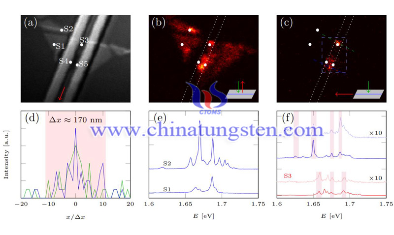
Researchers transferred the mechanically stripped WSe2 flakes onto a single-mode SiN, and after the transfer, the samples were placed in an optical cryostat of Montana instrument and cooled to 3.9 K. Photoluminescence (PL) from WSe2 can be either coupled to free space radiation or coupled to a guided mode. Radiation into the free space is collected by the top objective lens (numerical aperture NA is 0.65), while the PL coupled to the waveguide is captured by the lens fiber aligned with the output side.

All in all, the researchers realized the coupling of the quantum emitter to the waveguide by integrating the monolayer of WSe2 into the SiN chip. Single-photons are emitted with a waveguide-coupled saturation count rate of 100 kHz. That is, strain-induced quantum emitters could be coupled to photonic structures. A numerical analysis on the optimization of single photon extraction and indistinguishability using integrated dielectric cavity-emitter systems indicates that near-unity single-photon extraction can be achieved, even for low quantum yield emitters. It is a crucial step for the fundamental quantum photonics and 2D materials.
- Tungsten Manufacturer & Supplier, Chinatungsten Online: www.chinatungsten.com
- Tungsten News & Prices of China Tungsten Industry Association: www.ctia.com.cn
- Molybdenum News & Price: news.molybdenum.com.cn
- Tel.: 86 592 5129696; Fax: 86 592 5129797; Email: sales@chinatungsten.com


 sales@chinatungsten.com