Physicists Study Light Propagation in 2D Molybdenum Diselenide

light polarization spatial distribution image

An international research team has studied how light propagation in the plane of the thinnest semiconductor crystal in the world. It is found that the spatial distribution of light polarization is similar to that of three-color rapana.

The research results open the door for the development of monatomic optical transistors - quantum computer components can be calculated at the speed of light. The study was published in Nature Nanotechnology. At present, photons are considered to be most suitable for transmitting information in quantum computers. These computers are still hypothetical, based on the laws of the quantum field, and can solve some problems more effectively than the most powerful supercomputers.

"I expect that in the near future, two-dimensional monatomic crystals will be used to transmit information in quantum devices," said Professor Alexey Kavokin, director of the Spin Optics Laboratory at St. Petersburg University.

Classical computers and supercomputers take a long time to complete, and quantum computing devices will be completed soon. That's the great danger of quantum technology - as dangerous as the atomic bomb. For example, with their help, bank protection systems can be cracked very quickly. That's why intensive work is under way today, including the creation of a means to protect quantum devices: quantum cryptography. Our work contributes to semiconductor quantum technology.

light polarization spatial distribution image 1

light polarization spatial distribution image 2

At present, it is impossible to achieve this state at temperatures above - 70 C. However, once suitable materials are found, the invention will enable power to be transmitted to any point on the earth without any loss, and develop a new generation of motors.

In March 2018, Alexey Kavokin's team predicted that the structure of superconducting metals such as aluminium could help overcome this challenge. At present, researchers at the University of St. Petersburg are trying to find ways to obtain theoretical and experimental evidence.

Molybdenum Disulphide Transistors Direct Tailoring After-Fabrication

MoS2 image

Making electronic devices from exfoliated 2-D materials can be tricky. The Daniel Granados team of IMDEA Nanociencia designed a solution that includes post-fabrication customization of MOS 2-FET transistors using pulsed focused electron beam-induced etching.

Transition metal disulfides are thin layers of 2-D atoms bound together by Van der Waals force. These materials exhibit thickness-dependent variations in their physical properties and can be used in different optoelectronic applications.

Atomic thin layers of MoS2 can be separated by micromechanical stripping, but manufacturing optoelectronic devices from mechanically stripped MoS2 is a complex process. Even with the deterministic stamping method, the geometry of the device is limited by the flake shape in all cases. Even when CVD (Chemical Vapor Deposition) technology is used, device fabrication is hindered by materials growing in the island, which have reduced size and different physical properties.

Therefore, it is very interesting to develop the technology of customizing device geometry after the manufacturing step is completed. The group of Prof. Daniel Granados at IMDEA Nanociencia proposed an intelligent solution by modifying the geometry of several field-effect transistors (FET) made of exfoliated MoS2. The proposed method uses focused electron beam induced etching (FEBIE) and pulsed electron beam variation. The beam uses a pattern generator to scan the surface into a designed geometry, modify the conduction channel between the source and drain of the transistor, and allow customized device performance.

MoS2 image

Compared with the method using multiple manufacturing steps, this method has several advantages. First, it combines patterning and etching in one step rather than two-step nanofabrication. Secondly, it allows electronic and optical characterization before and after customization steps in a simple scheme. Lastly, pulsed FEBIE is a chemical method whose electron beam energy is lower than that of other studies (2.5 kV), which can reduce sample damage and prevent the distortion of MoS2 lattice. Because of these advantages, Granados et al. proposed nanoscissors. It is a significant alternative to expensive and time-consuming nanofabrication technologies, and has great potential for customization of post-fabrication with electrical and geometric characteristics of electronic and photoelectric devices.Making electronic devices from exfoliated 2-D materials can be tricky. The Daniel Granados team of IMDEA Nanociencia designed a solution that includes post-fabrication customization of MOS 2-FET transistors using pulsed focused electron beam-induced etching.

Transition metal disulfides are thin layers of 2-D atoms bound together by Van der Waals force. These materials exhibit thickness-dependent variations in their physical properties and can be used in different optoelectronic applications.

Atomic thin layers of MoS2 can be separated by micromechanical stripping, but manufacturing optoelectronic devices from mechanically stripped MoS2 is a complex process. Even with the deterministic stamping method, the geometry of the device is limited by the flake shape in all cases. Even when CVD (Chemical Vapor Deposition) technology is used, device fabrication is hindered by materials growing in the island, which have reduced size and different physical properties.

Therefore, it is very interesting to develop the technology of customizing device geometry after the manufacturing step is completed. The group of Prof. Daniel Granados at IMDEA Nanociencia proposed an intelligent solution by modifying the geometry of several field-effect transistors (FET) made of exfoliated MoS2. The proposed method uses focused electron beam induced etching (FEBIE) and pulsed electron beam variation. The beam uses a pattern generator to scan the surface into a designed geometry, modify the conduction channel between the source and drain of the transistor, and allow customized device performance.Compared with the method using multiple manufacturing steps, this method has several advantages. First, it combines patterning and etching in one step rather than two-step nanofabrication. Secondly, it allows electronic and optical characterization before and after customization steps in a simple scheme. Lastly, pulsed FEBIE is a chemical method whose electron beam energy is lower than that of other studies (2.5 kV), which can reduce sample damage and prevent the distortion of MoS2 lattice. Because of these advantages, Granados et al. proposed nanoscissors. It is a significant alternative to expensive and time-consuming nanofabrication technologies, and has great potential for customization of post-fabrication with electrical and geometric characteristics of electronic and photoelectric devices.transistors image

Electrochromic Tungsten Oxide Smart Glass Research or Boosting Fuel Cells Evolution

the researchers specifically studied electrochromic tungsten-oxide nanoparticles image

Recent research has found that electrochromic tungsten oxide smart glass plate research or providing new ideas for fuel cells research and development. Smart glass is an energy-efficiency product found in newer windows of cars, buildings, and airplanes, slowly changes between transparent and tinted at the flip of a switch.

Read more...

Rare Earth Exports to America Declined in Sino-US Trade War

China reduced rare earth exports to the US in June image

China's rare earth exported to the United States in June fell by 3.9% from May, reported by Reuters on July 27 that according to relevant Chinese customs data in last Saturday. The outside world suspects that Beijing has reduced exports to US as part of the Sino-US Trade War with the United States.

Read more...

Tungsten Carbide-Based Industry in Dongguan Introduces Talents

tungsten carbide rollers image

Tungsten carbide-based industry in Dongguan city has introduced high-level at home and abroad talents. According to the report of Yingmin Li, Chun Li of China News Service, 2019 high-level talents at home and abroad were held on July 24 in Guangdong. The person with ability is from the United States, Singapore, New Zealand, and other countries successfully signed 7 key talent projects, 9 intentions to settle projects of high-tech enterprises, new research and development institutions, and venture capital institutions.

Read more...

Tungsten Market Will be Profitable From Automobile & Aircraft Industry

aircraft manufacturing image

The tungsten market is expected to grow exponentially in the forecasting period. Overall, the increased demand for aircraft and the continuous application of tungsten alloys in the automotive sector will enhance the tungsten market valuation, which is expected to exceed $8.5 billion by 2025.

Due to the continuous demand of users for a wide range of applications, the global tungsten market has diffused from key characteristics of metals, such as corrosion resistance, wear resistance and flexibility. The metal is very important in the production of stellites, super alloys and heavy metal alloys for many parts such as automobiles, aircraft, gamma and X-ray machines, golf clubs, darts and so on. Consumer spending on automobiles, tourism and leisure activities, as well as increased health care services, will inadvertently increase demand for the tungsten market. The expansion of tungsten market will be promoted by factors such as increasing global steel consumption and aircraft production.

aircraft manufacturing image

Airbus said in its forecast that the future of the aviation industry is very optimistic and that more than 37,400 new freight and passenger aircraft will be needed in the next 20 years. These aircraft, worth nearly $5.8 trillion, represent the global growth of tourism and the rich prospects of the tungsten market and other ancillary market segments. The same report also pointed out that, despite any external factors affecting the aerospace sector, air traffic has increased over the past two decades and is expected to almost double in the next 15 years or so. Global gross domestic product (GDP) is considered a prominent indicator of expanding aviation growth. It is expected that 50% of air traffic growth will be triggered in the Asia-Pacific region, while the United States and Europe will together account for 30% of the growth.

To demonstrate the growing demand for aircraft, Boeing signed an agreement in November 2018 to sell about 300 aircraft to China, worth $37 billion, mostly for fleet growth. Similar contracts between airlines and global aircraft manufacturers will bring huge returns to the tungsten market. In addition to strengthening the review of aircraft performance and component quality, the tightening of international standards will affect the development of tungsten market.aircraft image

Investigation on Extracting Rare Earth From Coal

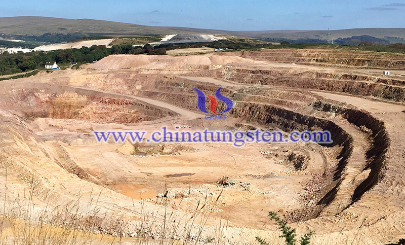
coal image

Geoscience BC, a geosciences research and data company in British Columbia, Canada, has some ideas on how to increase the supply of rare earth elements (REE): coal deposits and coal tailings facilities.

Geoscience BC has neither released information on its project financial investment nor how long its work will take. However, officials did say that BC coal bed may be a viable source of these elements, so its research will include characterization and quantification of REE and its extraction possibilities.

During the "Characterization and Extraction of Rare Earth Elements in East Kootenay Coalfield-REE BC Coal Project", the team will examine the samples, complete the characterization stage, and then test the potential extraction process on a laboratory scale.

coal image

The researchers added that in the first stage, they would develop a REE database, and they would prepare samples; in the second stage, they would go into the testing part of advanced characterization.

"With the advent of clean energy and defense technologies, the consumption of rare earth elements has increased rapidly," said Maria Holuszko, project leader.

"Traditional rare earth deposits are being rapidly depleted and are expected to meet demand only in the next 15 to 20 years," she said.coal deposits image

High Demand for Rare Earth Materials Promotes a Robust CAGR of 7% From 2018 to 2025

neodymium magnet image

London, July 23, 2019/AP-PR Newswire/Frost & Sullivan's latest analysis, Global Rare Earth Material Market, forecasts that by 2025, global growth in infrastructure development and e-Car demand is the key factor driving global growth of 5.4 billion U.S. dollars in rare earth materials. In China, Japan, Korea, the United States, Brazil and Western Europe, the demand for neodymium magnets, lanthanum and cerium based applications has increased, and the need for rare earth materials in metallurgical and battery applications has increased. Frost & Sullivan expects the market to grow at a strong CAGR of 7.0% from 2018 to 2025.

"There is a great demand for rare earth materials, especially for the production of high-end permanent magnets. The demand is characterized by niche requirements - high purity, professional rare earth material products, with extremely personalized application characteristics. The electronics, technology and automotive industries prefer these products, even if they are expensive to purchase," said Ganesh Dabholkar, senior analyst, chemicals & materials in infrastructure & mobility.

"Despite significant growth prospects, the rare earth material market is constrained by China's dominant position in reserves, product supply, project investment and consumption," Dabholkar pointed out. "There is an increasing trend in the extraction and use of rare earth materials, as well as in the research of alternative materials, recycling or the search for other low-cost rare earth products, which further hinder the growth of the market."neodymium magnet image

Beijing Institute of Technology 3D Printing Molybdenum Ion Thruster Components

3D printer image

Researchers in Beijing Institute of Technology are exploring better ways to identify ionic optics by adding materials to make molybdenum components. Their results have recently been published in the paper “3D Printed molybdenum for grids and keeper electrodes in ion thruster”.

The main components of ion thruster are ion optics and protector. Optics plays an important role in the geometry of the engine. However, their erosion limits the life of ion thrusters. The purpose of the protector is to protect the hollow cathode from "ion bombardment" and turn on the cathode discharge. Metals and carbon materials are usually used to make the necessary electrodes. Molybdenum is a metal material commonly used in ion optics and conservative manufacturing.

unsintered powder image

Among carbon-based materials with near zero thermal expansion coefficients (CTE) and lower sputtering yield than molybdenum, graphite has become a conventional choice because of its low cost and high understanding of its manufacturing methods, although pyrolytic graphite and carbon-carbon composites have been used for many times in ion optical systems mounted on important thrusters, the researchers said.

In order to simplify the manufacture of ion optics system, a study was carried out by Beijing University of Technology, focusing mainly on the 3D printing of molybdenum on the parts of electric propeller. It is successful and still in the development stage. So far, several healthy electrodes have been produced. The researchers chose selective laser melting (SLM) for the project, mainly because of its ability to print metals and, of course, because of the level of accuracy it can provide, especially in aerospace. The commonly used metal materials are titanium, aluminum and stainless steel.

The research project of Beijing Polytechnic University has created several 3D printed ion optics components previously used in titanium to further study the concept of ion optics in the fabrication of additives. Another study measured energy density, involving: laser power; laser scanning speed; hatch spacing; layer thickness.

"The results show that the mechanical and thermal properties of SLM molybdenum are similar to those of solid metals when the energy density applied in the preparation process is close to the maximum energy density, thus producing refractories, i.e. about 300 Jmm-3. This fact is related to the porosity produced, which decreases with the increase of energy density. The researchers concluded. The sputtering corrosion behavior of selective laser melting materials has not been evaluated yet, but it must be studied before the components manufactured by the additives can meet the practical application of electric propulsion.

3D printer image

Chinese Tungsten Prices Took a Backward Step in July

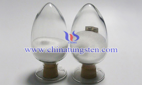
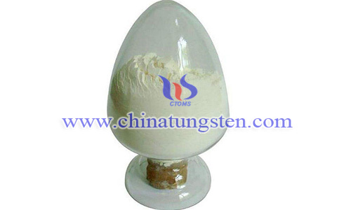
tungsten oxide image

Analysis of latest tungsten market from Chinatungsten Online

Chinese tungsten prices are unchanged from the previous trading day on persistent weakness in the demand side and uncertain outlook of the market. Most market participants take a watchful stance, waiting for further directions from large tungsten companies and institutions. 

Read more...


WeChat

Tungsten Metal

Tungsten Metal Price

Tungsten Alloy

Tungsten Alloy Price

Tungsten Carbide

Tungsten Carbide Price

Tungsten Powder

Tungsten Powder Price

Tungsten Copper

Tungsten Copper Price

Tungsten Oxide

Tungsten Oxide Price