100 Years of Doped Tungsten Wire Ⅲ - The Invention of Hard Metals
- Details
- Category: Tungsten Information
- Published on Wednesday, 13 July 2022 19:17
- Written by Caodan
- Hits: 1297
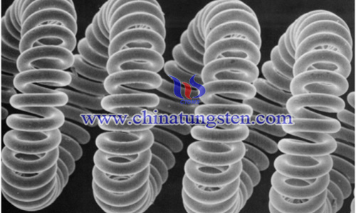
The Invention of Hard Metals
The next important milestone in the chronology of the development of doped tungsten wires is 1923, which marked the year when K. Schröter, chief engineer of the OSRAM research group in Berlin, Germany, made a cemented carbide or hard metal by combining tungsten carbide (WC) and cobalt powder through mixing, pressing and liquid-phase sintering.
Read more: 100 Years of Doped Tungsten Wire Ⅲ - The Invention of Hard Metals
100 Years of Doped Tungsten WireⅡ- The Coolidge Process
- Details
- Category: Tungsten Information
- Published on Wednesday, 13 July 2022 19:07
- Written by Caodan
- Hits: 1164
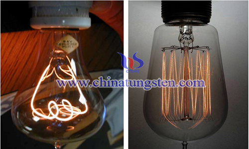
The Coolidge Process
William D. Coolidge (1873-1975), Figure 8, began his career at GE's research laboratory in September 1905. Interestingly, Coolidge's first task was to investigate the cause of the rapid breakage of the filament of the German tantalum lamp when operating under alternating current, most likely due to the limitations of the lamp's cavity technology and the residual gas in the bulb.
Read more: 100 Years of Doped Tungsten WireⅡ- The Coolidge Process
Six Tips for Caring and Clearing Tungsten Rings
- Details
- Category: Tungsten Information
- Published on Thursday, 23 June 2022 22:55
- Written by Caodan
- Hits: 1310
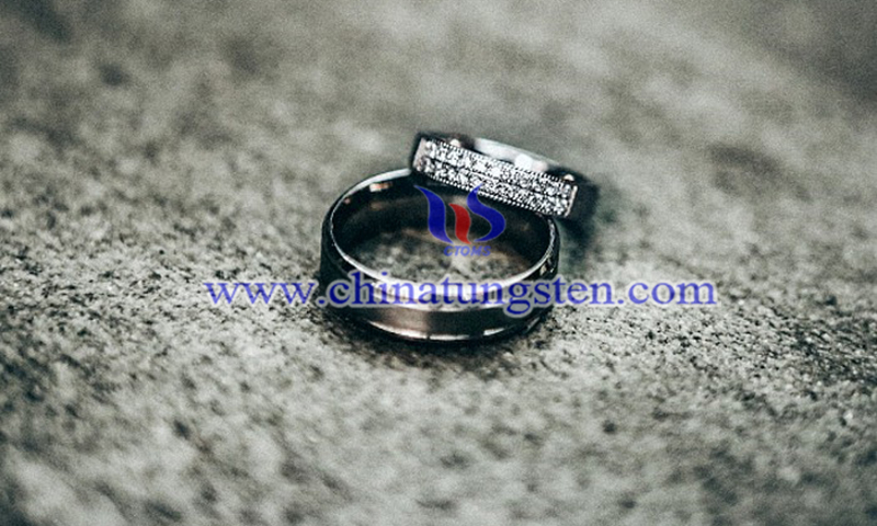
In recent years, tungsten rings have been a popular choice for their durable and scratch-resistant properties. However, they can also lose their luster over time. Below, we will explain how to take care of your tungsten wedding ring.
100 Years of Doped Tungsten WireⅠ- Early Attempts at Metallurgy
- Details
- Category: Tungsten Information
- Published on Wednesday, 13 July 2022 18:47
- Written by Caodan
- Hits: 1326
From a historical perspective, William D. Coolidge's development PM process and tool "for making tungsten ductile" in 1909 marked the beginning of the use of tungsten filaments in the lighting industry. William D. Coolidge's development of the PM process and tools to "make tungsten ductile" in 1909 marked a breakthrough in the use of tungsten filaments in the lighting industry and began the modern industrial era of Powder Metallurgy.
Read more: 100 Years of Doped Tungsten WireⅠ- Early Attempts at Metallurgy
Atomically MoS2 and WS2 Thin Semiconductors for Nanophotonics
- Details
- Category: Tungsten Information
- Published on Thursday, 23 June 2022 22:47
- Written by Caodan
- Hits: 1174
Atomically thin layers of semiconductors, such as molybdenum disulfide (MoS2) and tungsten disulfide (WS2), are promising materials for nanoscale photonic devices. These nearly two-dimensional semiconductor support so-called excitons or bound electron-hole pairs, which can be aligned vertically along the thin planes of the material.
Read more: Atomically MoS2 and WS2 Thin Semiconductors for Nanophotonics



 sales@chinatungsten.com