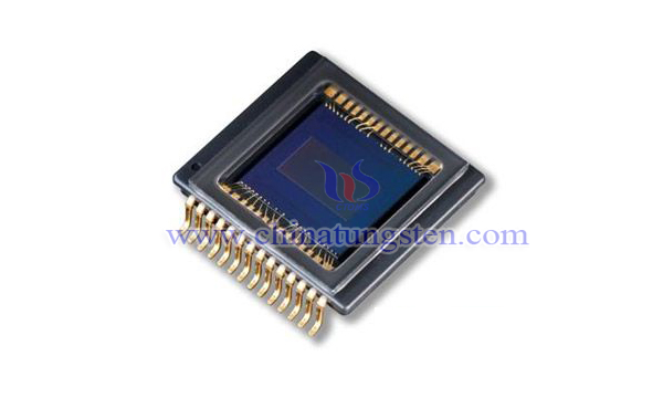
Metallic Tungsten Film Imaging Sensor Application
- Details
- Category: Tungsten Information
- Published on Sunday, 05 May 2019 20:56
With the development of semiconductor technology, the manufacture of camera sensor technology (CIS: CMOS image sensor) with metal oxide semiconductor technology has become a mainstream process in the field of emerging imaging. Among them, the metal film has a good visible light reflection conduction property, and is widely used as a reflection or isolation layer of incident light in the industry.

Metal tungsten film is used by most mainstream CIS manufacturers because of its excellent visible light reflection performance and good high temperature stability. However, it must be mentioned that the metal tungsten film used in CIS technology is not so good, and the difficulty is mainly due to the fact that the metal tungsten film is easy to form a high tensile stress due to its high temperature production process. The formation of such high tensile stress can easily cause micro-deformation of the whole wafer, which will seriously affect the quantity and quality of visible light transmission or isolation, and ultimately seriously affect the imaging quality of CIS products.
In order to overcome the tensile stress of the tungsten film, the researchers have lower the reaction temperature and reduce the amount of tungsten hexafluoride (WF6) gas, so that the tungsten film has lower stress than the conventional tungsten film. The specific technical solution is:
Titanium nitride is used as the semiconductor substrate, and the reaction gas is a gas containing tungsten hexafluoride (WF6) and hydrogen (H2). The temperature at which the gas is introduced into the reaction chamber to generate tungsten atoms is 395 °C - 450 °C. To ensure that as many tungsten atoms as possible are formed in the reaction chamber, rather than being formed on the surface of the semiconductor substrate. Finally, the atoms of the metal tungsten formed in the reaction chamber fall to the nucleation layer, and the crystal phase along the nucleation layer grows in an orderly manner, which is generated in situ instead of disorderly growth, and finally grows into a super Low stress metal tungsten film.
Metal tungsten film growth has strong adhesion growth characteristics, so the reaction temperature is increased to enhance the activation energy of the reaction; at the same time, the possibility of forming metal tungsten atoms on the surface of the semiconductor substrate is reduced by reducing the flow rate of the reaction gas, thereby maximizing the degree The metal tungsten atoms are formed in the reaction chamber instead of the disordered growth of tungsten atoms on the surface of the semiconductor substrate. In this way, the tensile stress problem of the metal tungsten film can be solved, and the tensile stress is estimated to be 73% less than that of the conventional method.
- Tungsten Manufacturer & Supplier, Chinatungsten Online: www.chinatungsten.com
- Tungsten News & Prices of China Tungsten Industry Association: www.ctia.com.cn
- Molybdenum News & Price: news.molybdenum.com.cn
- Tel.: 86 592 5129696; Fax: 86 592 5129797; Email: sales@chinatungsten.com


 sales@chinatungsten.com