How to Improve Tungsten Carbide Shield Cutter Properties?
- Details
- Category: Tungsten Information
- Published on Thursday, 07 May 2020 08:57
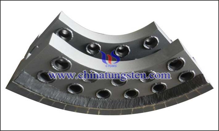
How to improve tungsten carbide shield cutter properties? Tungsten carbide has unique properties such as wear resistance, corrosion resistance, high hardness, and impact resistance, so it is often used to manufacture heads of cutters such as disc cutter, serrated knife or scraper for applying to a tunnel boring machine. While these cutters will inevitably break and wear. To improve service life of tungsten carbide cutters, some researchers have proposed a method to improve performance of tungsten carbide shield cutter.
Tungsten Carbide Shield Cutter
- Details
- Category: Tungsten Information
- Published on Thursday, 07 May 2020 08:56
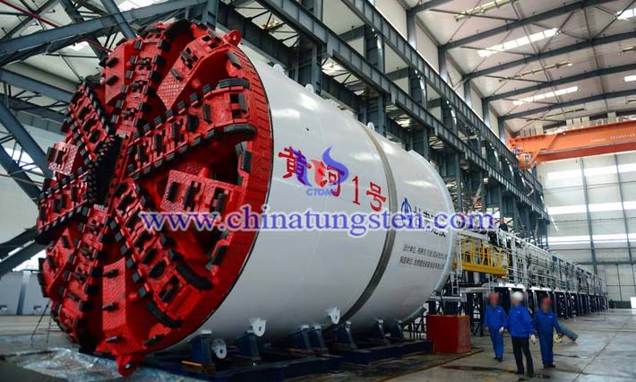
Tungsten carbide shield cutter is a type of tungsten carbide cutter applied for tunnel boring machines. Such a cutter is made of carbide materials (WC, TiC) of high hardness and high melting point, together with cobalt (Co), nickel (Ni) or molybdenum (Mo) as binding phase. Generally, the heads of these cutters is made of coarse-grained WC-Co cemented carbide.
Advantages of Tungsten Carbide Flowdrill
- Details
- Category: Tungsten Information
- Published on Tuesday, 05 May 2020 09:32
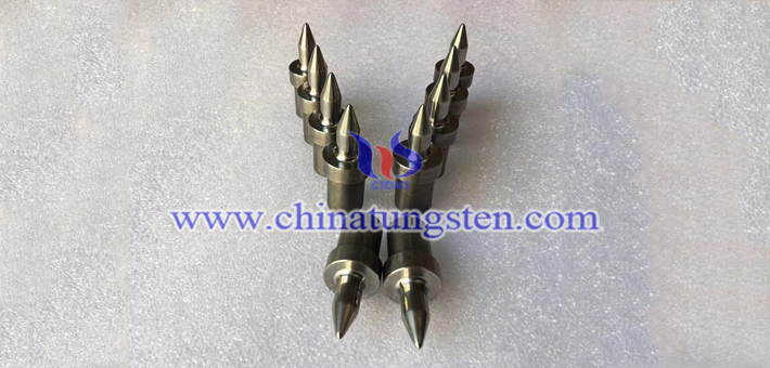
Tungsten carbide flowdrill is also called tungsten carbide fdrill that is environmentally friendly, wear resistant and high temperature resistant to drill hole with stability, high precision and beautiful surface. It provides a perfect solution for thin-wall drilling connection. Well, do you know what are advantages of tungsten carbide flowdrill?
Round Type Tungsten Carbide Flowdrill
- Details
- Category: Tungsten Information
- Published on Tuesday, 05 May 2020 09:30
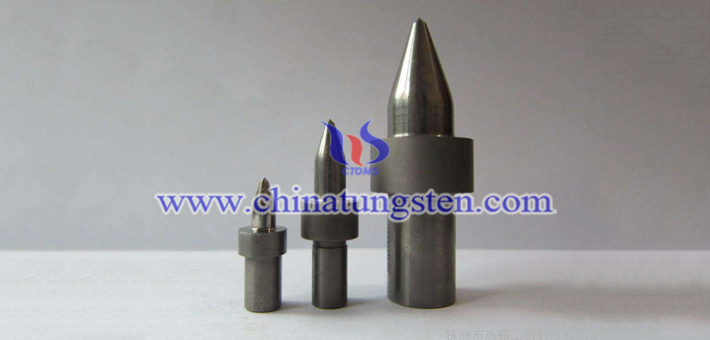
Round type tungsten carbide flowdrill is a standard flowdrill. The characteristic of the round type flowdrill made of high-quality tungsten carbide powder by certain processes is that the flowdrill penetrates the workpiece and stretches to form a bush while forming a convex ring on the surface of the workpiece. And the convex plate is suitable for thread sealing or nut washer.
Flat Type Tungsten Carbide Flowdrill
- Details
- Category: Tungsten Information
- Published on Tuesday, 05 May 2020 09:29
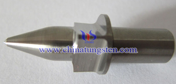
Flat type tungsten carbide flowdrill is a type of cemented carbide flowdrill that is divided according to the surface requirements of the workpiece. The characteristic of such a flat type flowdrill is that the flowdrill stretches through the workpiece to form a bush while cutting off the convex ring on the surface of the workpiece with smooth surface. Such a flowdrill is long lasting, stable and solid as the tungsten carbide is the most suitable raw material.
Working Principle of Tungsten Carbide Flowdrill
- Details
- Category: Tungsten Information
- Published on Tuesday, 05 May 2020 09:28
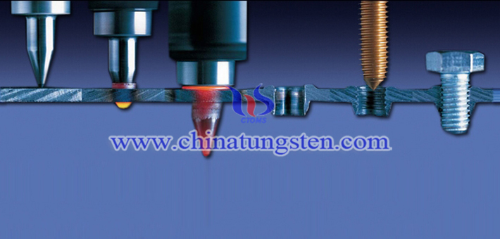
What is working principle of tungsten carbide flowdrill? You know, tungsten carbide flowdrill is a wear-resistant and high-temperature resistant drill bit for flowdrilling processes. The flowdrilling process is a chipless machining technology that processes holes and bushes on a metal sheet or tube at one time. Such a process has completely replaced the process of welding and riveting a nut on a thin-walled workpiece. Therefore, it is necessary for us to understand the working principle of flowdrill.
Welded Tungsten Carbide Drill Bit
- Details
- Category: Tungsten Information
- Published on Monday, 04 May 2020 19:07
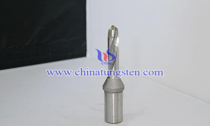
Welded tungsten carbide drill bit is composed of a steel drill body and a cemented carbide shank welded to the rear of the body. Adopting tungsten carbide powder and cobalt powder as raw materials, the drill bit is fabricated by cold pressing, vacuum sintering and other processes. The surface of the hole processed by such a drill bit has a good surface finish, high dimensional accuracy and positioning accuracy, and there is no need for subsequent finishing.
Tungsten Carbide Center Drill Bit
- Details
- Category: Tungsten Information
- Published on Monday, 04 May 2020 19:06
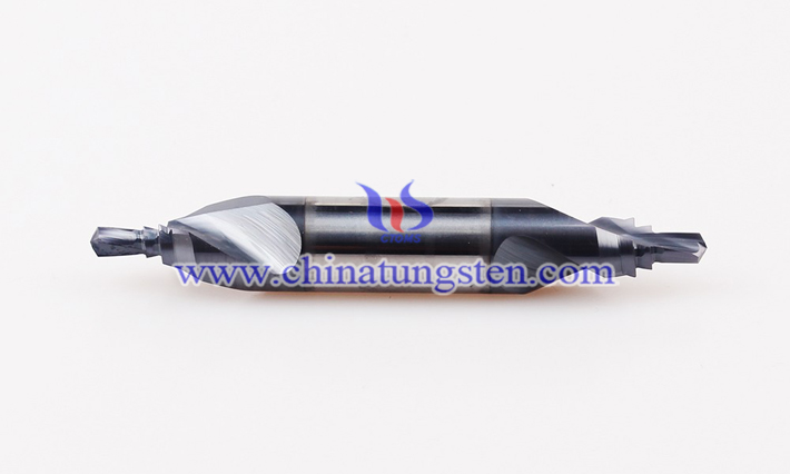
Tungsten carbide center drill bit is made of high quality tungsten carbide with the advantages of high hardness, wear resistance, corrosion resistance, high temperature resistance, etc., so that the drill bit has the advantages of accurate positioning, quick cutting, good chip removal, and high efficiency. And therefore the center drill bit is mainly used for center hole processing on the end faces of shafts and other parts. More specifically, it is mainly applied for precise positioning of prefabricated holes and guides twist drills for hole processing to reduce errors.
Tungsten Carbide Microdrill Bit
- Details
- Category: Tungsten Information
- Published on Monday, 04 May 2020 19:04
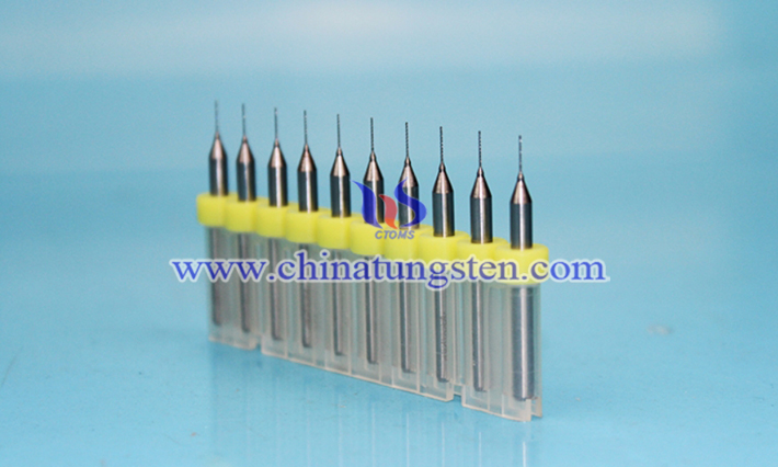
Tungsten carbide microdrill bit refers to a type of tungsten carbide drill bits having a diameter of less than 3.175 mm. In order to make the microdrill bit have an effective drilling effect, a series of factors must be considered: such as various elements of drill itself, processing parameters, hole depth, installation completeness, and the structure of workpiece.
Tungsten Carbide Hole Saw
- Details
- Category: Tungsten Information
- Published on Monday, 04 May 2020 19:03
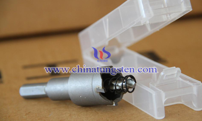
Tungsten carbide hole saw is a special drill bit for processing circular holes in modern industry or engineering. The hole saw is attached to a drill, and used to cut large holes in wood, plastic, plaster, organic glass, or metals such as copper, iron, and stainless steel.


 sales@chinatungsten.com