One-dimensional Tungsten Oxide-Vanadium Oxide Heterojunction Nanowire Arrays
- Details
- Category: Tungsten Information
- Published on Monday, 23 September 2019 21:52
- Written by meiwei
- Hits: 1335
The active atoms of tungsten oxide are located on the surface of the crystal, which greatly enlarges the contact area between the crystal surface and the gas, and can effectively improve the gas sensing performance. Tungsten oxide with one-dimensional nanowire structure attracts many researchers because of its huge specific surface area.

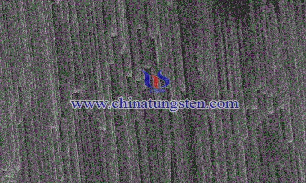
It has been proved that tungsten oxide with one-dimensional nanowire structure has indeed improved the sensitivity of gas detection, but it still needs to be modified by gas sensitive materials to improve gas sensitivity. The main ways are doping precious metals Pt, Au, Pd or transition metal oxides. In addition, they can be modified by constructing heterostructures. Compared with doped noble metals, heterojunction tungsten oxide materials have lower cost and are easier to push rice. Some scholars have developed a one-dimensional tungsten oxide-vanadium oxide heterojunction nanowire array. The preparation process includes the following steps:
Step 1: Tungsten thin films were deposited on the substrate by magnetron sputtering. Tungsten metal was used as target, inert gas was used as sputtering gas, sputtering pressure was 1-2.0 Pa, sputtering power was 80-110 W, sputtering time was 15-20 min.
Step 2: Tungsten oxide nanowires were grown by crystallization of tungsten thin films prepared in step 1 in a vacuum high temperature tube furnace. The ambient atmosphere was a mixture of oxygen and argon. During the growth of tungsten oxide nanowires, the flow rates of oxygen and argon were controlled to be 0.1 SCCM and 35-50 SCCM respectively. The growth pressure in the furnace was controlled to be 140-160 Pa. The furnace rises from room temperature 20-25 degrees Celsius to 600-700 degrees Celsius, the heating rate is 5 degrees Celsius/min, the temperature is kept at 600-700 degrees Celsius for 1-2 hours, then the temperature is lowered from 1 hour to 300-400 degrees Celsius, and finally the natural cooling to room temperature 20-25 degrees Celsius.
Step 3: After annealing, the tungsten oxide nanowires prepared in step 2 were annealed for 1-2 hours at 300-500 ℃ in air atmosphere to further stabilize the crystal orientation.
Step 4: Vanadium films were deposited on tungsten oxide nanowire layers prepared by magnetron sputtering on target after step 3. Vanadium metal was used as target material, inert gas was used as sputtering gas, the flow rate of inert gas was 30-50 sccm, the working pressure of sputtering was 2.0 Pa, the sputtering power was 80-110 W, and the sputtering time was 2-5 min.
Step 5: Annealing treatment of vanadium is carried out. The substrate of the deposited metal vanadium film obtained by step 4 treatment is annealed for 1-2 hours at 300-500 ℃ in air atmosphere.
The tungsten oxide-vanadium oxide heterostructure fabricated by the above method has a high specific surface area and can give full play to the advantages of the heterostructure. The response sensitivity of the heterostructure to 5ppm-grade NO2 gas at room temperature is 7-9 times that of the pure tungsten oxide nanowire, and the response time is less than 3s.
- Tungsten Oxide Manufacturer & Supplier, Chinatungsten Online: www.tungsten-oxide.com
- Tungsten News & Prices of China Tungsten Industry Association: www.ctia.com.cn
- Molybdenum News & Price: news.molybdenum.com.cn
- Tel.: 86 592 5129696; Fax: 86 592 5129797; Email: sales@chinatungsten.com


 sales@chinatungsten.com