Applications of Tungsten Wire in Glass Molding
- Details
- Category: Tungsten Information
- Published on Thursday, 26 June 2025 19:31
- Written by Zhenghua
- Hits: 217
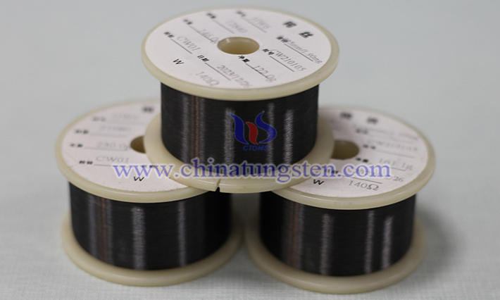
Tungsten wire is widely used in the industrial field, especially in the glass molding process, due to its high melting point, corrosion resistance and excellent mechanical properties. Tungsten wire is mainly used in key links such as heating, cutting and molding in glass manufacturing, and its unique properties can meet the needs of high temperature and complex process environments.
Application of Tungsten Wire in Glass Melting
- Details
- Category: Tungsten Information
- Published on Thursday, 26 June 2025 19:29
- Written by Zhenghua
- Hits: 209
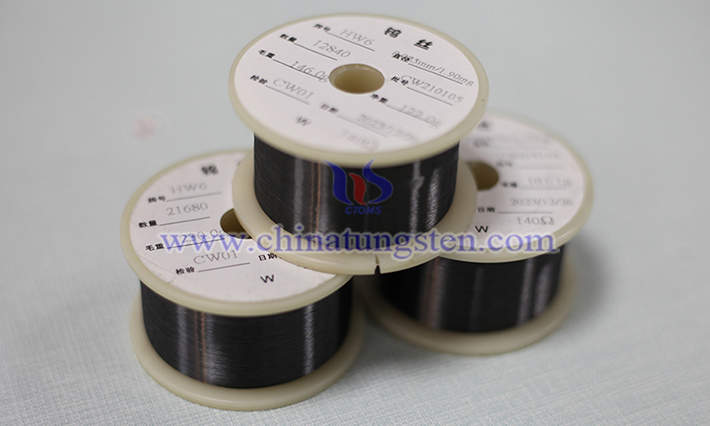
Tungsten wire has an indispensable application in the heating, molding and experiment of glass melting due to its excellent high temperature performance and chemical stability. It is a key material in modern glass industry and scientific research.
Advantages of Tungsten Wire in Heating Glass Process
- Details
- Category: Tungsten Information
- Published on Thursday, 26 June 2025 19:25
- Written by Zhenghua
- Hits: 193
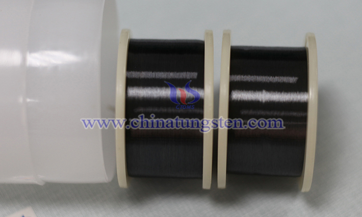
As a high-performance functional material, tungsten wire has shown multi-dimensional technological innovation value and application advantages in the field of heating glass process. Its unique physical and chemical properties not only break through the limitations of traditional heating technology, but also promote the evolution of glass products towards intelligence and efficiency.
Read more: Advantages of Tungsten Wire in Heating Glass Process
Design Principle of Tungsten Wire in Glass Heating Equipment
- Details
- Category: Tungsten Information
- Published on Thursday, 26 June 2025 19:27
- Written by Zhenghua
- Hits: 211
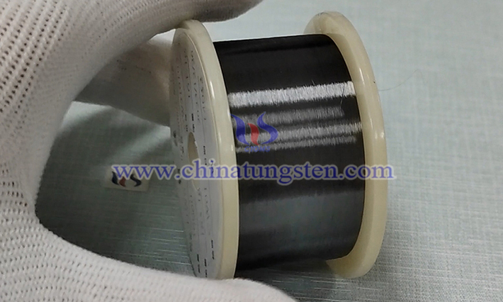
The core design of tungsten wire heating elements used in glass heating equipment (such as glass kilns, furnaces or vacuum coating equipment) is to use the extreme high temperature stability and efficient radiation heat transfer ability of tungsten metal to achieve uniform and rapid heating of glass in harsh environments. The following are its key design principles:
Read more: Design Principle of Tungsten Wire in Glass Heating Equipment
Selection of Tungsten Wire in Glass Heating System
- Details
- Category: Tungsten Information
- Published on Thursday, 26 June 2025 19:23
- Written by Zhenghua
- Hits: 194
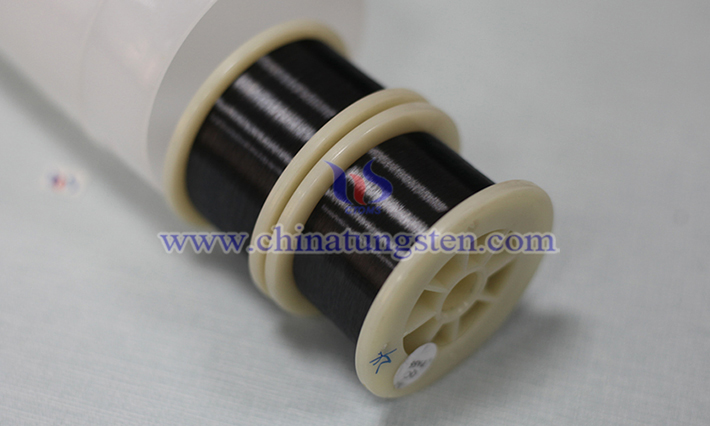
Tungsten wire has an extremely high melting point (about 3422℃) and is an ideal high temperature resistant material in glass heating system. Its resistivity is moderate, it can heat up quickly when heated, and it has good thermal stability and is not easy to deform or melt. Tungsten wire also has a low thermal expansion coefficient and can maintain structural stability at high temperatures. In addition, the chemical inertness of tungsten makes it difficult to react with glass or surrounding gases at high temperatures, extending its service life.
Read more: Selection of Tungsten Wire in Glass Heating System


 sales@chinatungsten.com