Using Lithography-Free Process to Create Quantum Emitters on Tungsten Diselenide
- Details
- Category: Tungsten's News
- Published on Tuesday, 07 June 2022 23:39
In a recent paper published in ACS Nano, researchers demonstrate a scalable, bottom-up, lithography-free process for creating large-area, dense quantum emitters on monolayers of tungsten diselenide (WSe2). In this study, the researchers placed a WSe2 monolayer on top of platinum (Pt) nanoparticles to induce strain within the WSe2 monolayer.
Physical confinement and strain engineering of three-dimensional (3D) semiconductors allow quantum information processing and bandgap engineering. Semiconducting transition metal dichalcogenides (TMDCs) and hexagonal boron nitride are the two-dimensional (2D) materials explored in this study.
The structural properties of 2D materials make them competitive strain engineering materials. The heterogeneous binding of 2D materials to arbitrary substrates containing optical/photonic nanostructures is due to their in-plane binding, which indicates the strain tunability of 2D materials through the substrate topology. Furthermore, silica-based nanopillars can be used as three-dimensional substrates to induce local strain.
![]()
(Source: klss/Shutterstock.com)
Since mechanical strain can control the band structure, they are used to modulate photonic and electronic properties. As a result, quantum emitter (QE) in TMDCs have received considerable attention in quantum information science and engineering as well as 2D nanophotonics, yet the origin of quantum emission from TMDCs remains unclear.
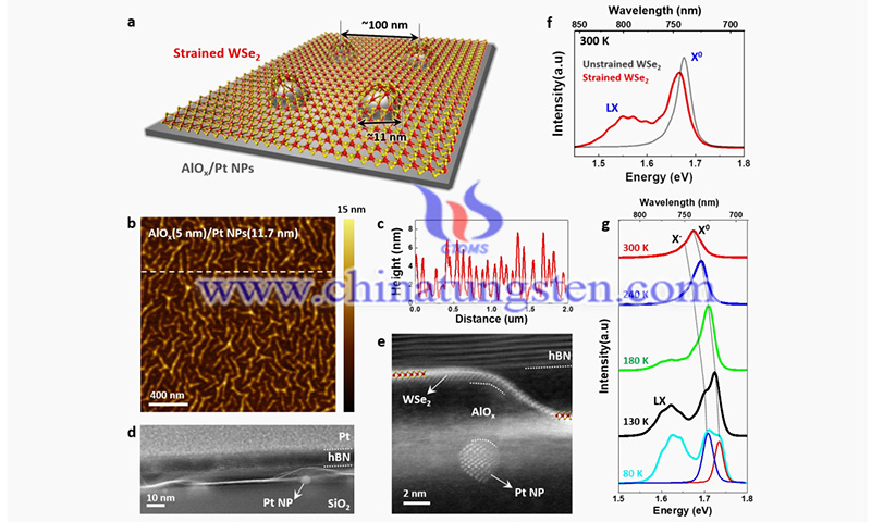
In this work, the authors demonstrate a method for forming highly dense, strain-induced quantum emitters in a two-dimensional TMDC monolayer placed on top of uniformly aligned metal nanoparticles using a lithography-free process, top-down alumina (AlOx) dielectric layer approach. By using far-field photoluminescence (PL) spectroscopy, they observed localized exciton (LX) emission from the strained WSe2 structure of platinum.
The team has understood the mechanism behind the LX emission from strained WSe2 through a comprehensive study of room temperature near-field and low-temperature far-field PL spectra. They observed that the origin of LX emission is radiative emission from dark excitons, controlled by compressive strain. The same LX emission was observed in a large area of WSe2 monolayers by metal-organic chemical deposition (MOCVD).
In addition, the spatial control of MOCVD was performed using platinum nanoparticles arranged in a burst of columns. Time-resolved and low-temperature PL measurements indicate a lifetime of about 11 ns and an emission spectral line width of less than 0.7 nm.

(Source: Kim, G./ACS nano)
First, a thin layer of alumina was deposited on uniformly aligned platinum nanoparticles laid on a substrate with the help of binary copolymer micelles. The platinum nanoparticles were spin-coated with a monolayer of polystyrene-block-poly(4-vinylpyridine) (PS-P4VP) micelles, and the platinum nanoparticle core consisted of hexachloroplatinic acid (H2PtCl6) precursor. Then, the nanoparticles were annealed at 400 degrees Celsius. The dimensions of the platinum nanoparticles were 11.7 and 5.9 nm, depending on the molecular weight of the binary copolymer.
In this study, nanoparticles with a size of 11.7 nm and an inter-particle distance of 103 nm were investigated. The AlOx layer was deposited on the platinum nanoparticles by atomic layer deposition (ALD) and was used as a spacer, which prevents the quenching of excitons in the 2D TMDC by direct contact with the platinum nanoparticles. In addition, the thicker alumina leads to a high difference between the substrate and the top of the platinum nanoparticles.
After ALD alumina deposition, the tungsten diselenide monolayer was transferred to the AlOx-deposited Pt-Au nanoparticle arrays. Finally, the synthesized samples were annealed in a vacuum tube furnace with an argon gas stream to provide better conformal contact at the interface between the alumina/platinum nanoparticle substrate and WSe2 and to eliminate trapped gas molecules or solvents.
Atomic force microscopy (AFM) and scanning transmission electron microscopy (STEM) were used to observe the structure of annealed, locally strained WSe2 on AlOx/platinum nanoparticle arrays. The results show distinct wrinkles between the nanoparticles, indicating strain and deformation of the WSe2 monolayer. STEM images and energy-dispersive X-ray spectroscopy (EDS) elemental maps show the WSe2 monolayer with alumina overlaid between the platinum nanoparticle arrays, suggesting the generation of locally strained structures.
In summary, the team demonstrated a facile method to fabricate localized quantum emitters with high spatial density by strain induction in tungsten diselenide monolayers distributed on uniform platinum nanoparticles.
A comprehensive strain was induced by the topology of the sample and the density of the platinum nanoparticles and by tuning the LX emission of the dark exciton. This study uses a lithography-free process and can be extended to large area TMDCs and applied to 2D semiconductors.
The study titled “High-Density, Localized Quantum Emitters in Strained 2D Semiconductors” has been published in ACS nano (2022). The study was carried out by Kim, G., Kim, H. M., Kumar, P., Rahaman, M., Stevens, C. E., Jeon, J., and Jariwala, D.
- Tungsten Manufacturer & Supplier, Chinatungsten Online: www.chinatungsten.com
- Tungsten News & Prices of China Tungsten Industry Association: www.ctia.com.cn
- Molybdenum News & Price: news.molybdenum.com.cn
- Tel.: 86 592 5129696; Fax: 86 592 5129797; Email: sales@chinatungsten.com


 sales@chinatungsten.com