Crystal Structure of Tungsten Disulfide
- Details
- Category: Tungsten Information
- Published on Monday, 22 August 2022 20:26
The crystal structure of tungsten disulfide (WS2) belongs to the P63/mmc space group with lattice parameters of a = 0.31532 nm and c = 1.2323 nm measured by X-ray diffraction. As a typical representative of two-dimensional layered transition metal dichloride (TMDC) materials with a structure consisting of 0.6-0.7 nm thick X-M-X interlayers (M is transition metal; X = S, Se, Te).
WS2 possesses a similar sandwich structure, with each sandwich plate consisting of three atomic layers (the middle layer is a W-atomic layer; both upper and lower layers are S-atomic layers), forming an S-W-S structure.

The atoms within each layer are connected by ionic bonds, where covalent interactions contribute significantly, and adjacent tungsten disulfide interlayers are bonded by van der Waals forces. The distance between adjacent layers is about 0.65 nm, which is higher than that of graphite (0.33 nm), which can provide space for ion embedding and extraction.
According to the stacking form, the crystal structure of WS2 can be divided into three types: a one-layer stacked trigonal 1T-WS2, a two-layer stacked hexagonal polycrystalline 2H-WS2, and a three-layer stacked rhombohedral 3R-WS2, where T, H, and R represent trigonal, hexagonal and rhombohedral shapes, respectively, and the numbers indicate the number of layers in a cell. Among them, 1T-WS2 consists of six sulfur atoms with tungsten atoms in the center, and the crystal structure of 1T-WS2 is formed by repetitive stacking in a single manner in a single manner.
The electrical conductivity of 1T-WS2 (metallic phase) is about 105 times higher than that of 2H-WS2, which makes it more competitive for electrochemical applications. Unfortunately, the application of 1T-WS2 is limited by its fickleness, and the 1T phase may transform to 2H phase at high temperatures (~95-100°C). 2H-WS2 (semiconductor phase) exhibits a hexagonal polyhedron, with each sandwich plate consisting of a shared trigonal prism and tungsten atoms located at the center.
Different from 1T-WS2, the sulfur atoms in 2H-WS2 are antiparallel to the sulfur atoms of the adjacent layers from one layer so that one cell contains two sandwich plates. 2H-WS2 is naturally stable, has lower conductivity than 1T-WS2, and exhibits semiconductor properties. In 3R-WS2, the trigonal prisms of adjacent layers are arranged parallel to each other. However, only every fourth layer is aligned with the first layer.

Thus, the cell contains three S-W-S layers. 3R-WS2 is the least studied polycrystalline type because it has nearly insulating properties. Methods to study the electronic band structure of WS2, both bulk and nano WS2, can be divided into two categories: experimental studies based on various optical absorption spectroscopy techniques and theoretical calculations based on density flooding theory (DFT). Experimentally, it can be studied directly by photoelectron spectroscopy (PES).
In PES, electrons on the sample surface are excited by photons and escape from the surface, and information about the occupied state can be revealed by detecting the measurement of the electron energy distribution. In addition, angle-resolved photoelectron spectroscopy (ARPES) is an improved characterization method that combines PES with high energy resolution, high angular resolution, and ultra-high vacuum technology.
In terms of theoretical calculations, various theoretical approaches have also been used to study the electronic band structure of WS2. Most studies have used local density (LDA) or generalized gradient approximation (GGA) based on the Kohn-Sham density functional theory (KS-DFT). However, KS-DFT using LDA suffers from a well-known problem in that the band gap is usually underestimated relative to the fundamental band gap measured from experiments.
Up to now, researchers have conducted a lot of studies on the electronic band structure of bulk and nano WS2. Regarding the bulk WS2, some researchers have obtained the ionization potential value of WS2 from PBE as 5.14 eV, while only very few experimental data exist about the ionization potential of WS2.
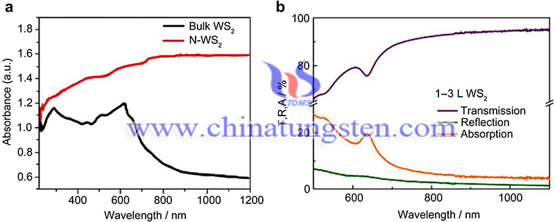
Due to the insufficient band gap (the thermodynamically required band gap has a minimum value of 1.23 eV), the bulk tungsten disulfide materials are not suitable as photocatalysts for water separation. Therefore, increasing the band gap to enhance the application of WS2 in electrocatalysis and photocatalysis is an important research direction. When WS2 is fabricated into nanostructures, the band gap can be widened, which is attributed to the quantum confinement and edge effects of WS2. Since the band gap is the energy between the conduction band minimum (CBM) and the valence band maximum (VBM), the band position of WS2 can also be tuned.
Article Source: Sun, CB., Zhong, YW., Fu, WJ. et al. Tungsten disulfide-based nanomaterials for energy conversion and storage. Tungsten 2, 109–133 (2020).
- Tungsten Manufacturer & Supplier, Chinatungsten Online: www.chinatungsten.com
- Tungsten News & Prices of China Tungsten Industry Association: www.ctia.com.cn
- Molybdenum News & Price: news.molybdenum.com.cn
- Tel.: 86 592 5129696; Fax: 86 592 5129797; Email: sales@chinatungsten.com


 sales@chinatungsten.com