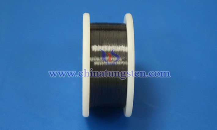
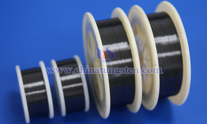
Cut-Resistant Tungsten Wire: Ideal for Zero Edge Chipping Cuts
- Details
- Category: Tungsten Information
- Published on Thursday, 03 April 2025 19:10
In the field of precision manufacturing, the accuracy and quality of material cutting directly impact the performance and lifespan of end products. Traditional cutting materials often struggle with issues like edge chipping and debris when processing high-hardness or brittle materials, leading to reduced yield rates. The introduction of CTIA GROUP’s cut-resistant tungsten wire offers a revolutionary solution to this challenge.
I. The Edge Chipping Problem: The Hidden Threat in Precision Manufacturing
In applications such as semiconductor wafer dicing, sapphire substrate processing, and photovoltaic silicon wafer cutting, even minor edge chipping can trigger a cascade of issues:
Performance Degradation: Edge chipping causes stress concentration, reducing the material’s mechanical strength.
Yield Loss: Optical components, sensors, and similar products may require rework or scrapping.
Cost Increase: Additional grinding and inspection steps increase production costs and slow efficiency.
Traditional cutting wires (e.g., copper or steel wires) often lack sufficient toughness or fail to control the heat-affected zone (HAZ), making it difficult to balance efficiency and precision. Cut-resistant tungsten wire, however, breaks through this bottleneck.

II. Core Advantages of Cut-Resistant Tungsten Wire: A Breakthrough in Material and Process
1. Exceptional Strength and Toughness
Tungsten boasts a tensile strength exceeding 3,500 MPa—six times that of ordinary steel wire. Its unique body-centered cubic lattice structure provides outstanding impact resistance, effectively absorbing fracture energy during the cutting of hard, brittle materials and physically suppressing edge chipping.
2. Precise Heat-Affected Zone Control
With a melting point of 3,422°C, cut-resistant tungsten wire heats up slowly and uniformly during cutting. When paired with pulsed power technology, it enables nanoscale control of the cutting kerf. Experimental data shows that the heat-affected layer thickness in tungsten wire cutting can be kept below 5 μm—far less than the 30 μm typical of traditional methods.
3. Dynamic Stability and Longevity
The surface of cut-resistant tungsten wire is treated with a nano-coating, reducing the friction coefficient by 40%. Combined with diamond grinding wheel assistance, a single tungsten wire can exceed 500,000 cutting cycles, lowering overall costs by 35%.

III. Application Scenarios: Redefining the Boundaries of Precision Processing
1. Semiconductor Wafers
Traditional Challenge: Edge chipping leads to chip failure.
Tungsten Wire Solution: Edge chipping rate <0.1%, supports 12-inch wafer cutting.
2. Photovoltaic Silicon Wafers
Traditional Challenge: High cutting loss and debris rates.
Tungsten Wire Solution: Thin slicing (<100 μm) with a 60% increase in yield rate.
3. Sapphire and Ceramics
Traditional Challenge: Edge microcracks impair light transmission.
Tungsten Wire Solution: “Zero edge chipping” cutting, achieving Ra roughness of 0.2 μm.
IV. Aerospace
Traditional Challenge: Delamination in carbon fiber composites.
Tungsten Wire Solution: Low-damage cutting, preserving the material’s original mechanical properties.
- Chinatungsten Online: www.tungsten.com.cn
- CTIA GROUP LTD: en.ctia.group
- Tungsten News & Price: www.ctia.com.cn
- Molybdenum News & Price: news.molybdenum.com.cn
- Tel.: 86 592 5129696; Email: sales@chinatungsten.com


 sales@chinatungsten.com