Sapphire Dan Changjing Tungsten Crucible Furnace
- Details
- Category: Tungsten & Sapphire Growth Furnace News
- Published on Tuesday, 11 March 2014 15:22
- Hits: 2611
First, Sapphire tungsten crucible furnace Dan Changjing About Sapphire Dan Changjing tungsten crucible furnace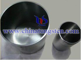
Sapphire Dan Changjing tungsten crucible furnace is one of tungsten products, mainly divided sintering ( applied to the powder metallurgy technique ) , stamping , spinning type . Turning the use of tungsten rod shape ( generally relatively small size ) , forming a variety of welding , the use of pure tungsten plate , tungsten film processing and pure tungsten rod made by the corresponding process . Sapphire Dan Changjing tungsten crucible furnace using an inert gas in a vacuum degrees in 2600 . The melting point of the high boiling point of tungsten , high temperature strength , wear resistant , high thermal conductivity , low coefficient of thermal expansion , good hardenability . Widely used in the tungsten crucible smelting of rare earth , quartz glass, electronic spraying, and other crystal growth sectors .
Tungsten melting point, high boiling point , high temperature strength , anti-friction , corrosion resistance, high thermal conductivity , low coefficient of thermal expansion , good hardenability , thanks to such excellent properties, are widely used in a tungsten crucible smelting of rare earth , quartz glass, electronic spraying , crystal growth and other industries.
Second, Sapphire Dan Changjing tungsten crucible furnace physical and chemical properties
1 Purity : W ≥ 99.95%;
2 , Density : ≥ 18.5g/cm3;
3, The maximum application temperatures : 2400 ℃.
Third, Sapphire Dan Changjing tungsten crucible furnace uses
Since the melting point of tungsten 3410 ℃, and therefore is widely used in the tungsten crucible core container sapphire single crystal growth furnace , quartz glass melting furnace, the rare earth and other industrial furnace, smelting furnace , the use of working temperatures generally above 2000 ℃. Especially for sapphire single crystal growth furnace , the high purity , high density, without internal cracks, precise size , smooth inner and outer walls , and other features of the tungsten crucible for sapphire crystal growth process seed success rate , pulling quality control, from crystal stick pan and life has played a key role.
Tungsten Manufacturer & Supplier: Chinatungsten Online - http://www.chinatungsten.com
Tel.: 86 592 5129696; Fax: 86 592 5129797
Email: sales@chinatungsten.com
Tungsten & Molybdenum Information Bank: http://i.chinatungsten.com
Tungsten News & Tungsten Prices, 3G Version: http://3g.chinatungsten.com
Molybdenum News & Molybdenum Price: http://news.molybdenum.com.cn
What Is A Sapphire?
- Details
- Category: Tungsten & Sapphire Growth Furnace News
- Published on Tuesday, 11 March 2014 13:34
- Hits: 2637
Sapphire (Sapphire) is an alumina (Al2O3) single crystal , the optical penetration with a wide range from the near UV (190nm) to 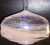 the infrared lens has good optical properties of single crystal alumina . Sapphire crystal has excellent optical properties, mechanical properties and chemical stability , high strength , hardness , corrosion resistance, can work in temperatures close to 2000 ℃ harsh conditions , they have been widely used in military infrared devices , satellite space technology, high-intensity laser window materials . Its unique lattice structure , excellent mechanical properties , good thermal properties make sapphire crystal semiconductor GaN/Al2O3 become practical light-emitting diode (LED), LSI SOI and SOS nanostructured superconducting films and the most ideal substrate material . With the recent LED TV, LED Monitor, LED NB, sustained high growth LED Phone and LED lighting market , driven by strong demand for the production of LED sapphire substrate market expansion.
Since tungsten and molybdenum has a high temperature , low pollution and other characteristics, are widely used to make Sapphire Dan Changjing furnace hot zone components, including tungsten crucible / molybdenum crucible , heating element , tungsten tube, heat shield, support base, the seed rod , the crucible cover. Heating element cage structure using tungsten or tungsten mesh heating element heating element , help provide a uniform and stable temperature field .
Tungsten Manufacturer & Supplier: Chinatungsten Online - http://www.chinatungsten.com
Tel.: 86 592 5129696; Fax: 86 592 5129797
Email: sales@chinatungsten.com
Tungsten & Molybdenum Information Bank: http://i.chinatungsten.com
Tungsten News & Tungsten Prices, 3G Version: http://3g.chinatungsten.com
Molybdenum News & Molybdenum Price: http://news.molybdenum.com.cn
Improving Light-Emitting Diode Performance through Sapphire Substrate Double-Side Patterning
- Details
- Category: Tungsten & Sapphire Growth Furnace News
- Published on Monday, 10 March 2014 15:09
- Hits: 2701
Here, we present a new double-side patterned sapphire substrate methodology that improves the efficiency of gallium  nitride-light emitting diodes (GaN-LEDs). The light extraction efficiency of GaN-based LEDs was analyzed through the use of a ray-tracing simulation. The extraction efficiency was simulated using patterned sapphire substrate LEDs with a variety of shapes, depths, sizes, and spacing. Through the optimal patterning of the various factors, high extraction efficiency was realized and subsequently improved upon. The thermal LED characteristics were analyzed through the use of the COMSOL general heat transfer module. The LEDs patterned on the sapphire substrate were fabricated using nano imprint lithography. We found that the output power of the double-side patterned LED was 52% greater than that of a flat LED. The thermal resistance of the double side patterned LED was 9.5 K/W less than that found for the flat LED.
As the lighting industry continues to advance, the light emitting diode (LED) market share is increasing explosively. The biggest reason for this growth is that LEDs are more energy efficient and have a longer life compared with conventional light sources. The era of full-scale LED applications has arrived as blue and white gallium nitride (GaN) semiconductor based LEDs are commercialized. The LEDs offer the benefits of fast processing speed of a semiconductor and low electricity consumption. As such, they have been accepted into the strategic national product for green growth. The development of the blue GaN LED in the mid-1990s enabled the full-color LED displays that have become a common feature in our daily lives. The high intensity LED market is expanding too fast to measure; efforts to enlarge the chips, improve their luminous efficiency, and the enhancement of their heat dissipation technology support are actively ongoing. However, LEDs have their own problems. The biggest problem is that LED prices are 20 times more expensive than conventional lighting; this is a big burden for their use in households and offices. In order to develop low cost, high intensity LEDs for lighting, more studies regarding luminous efficiency improvement and heat dissipation system development are needed.
Tungsten Manufacturer & Supplier: Chinatungsten Online - http://www.chinatungsten.com
Tel.: 86 592 5129696; Fax: 86 592 5129797
Email: sales@chinatungsten.com
Tungsten & Molybdenum Information Bank: http://i.chinatungsten.com
Tungsten News & Tungsten Prices, 3G Version: http://3g.chinatungsten.com
Molybdenum News & Molybdenum Price: http://news.molybdenum.com.cn
Sided Patterned Sapphire Substrate to Improve Research Performance of Light-Emitting Diodes
- Details
- Category: Tungsten & Sapphire Growth Furnace News
- Published on Monday, 10 March 2014 15:22
- Hits: 2533
There have been many studies regarding increased LED efficiency. The patterned sapphire substrate (PSS) method has been  reported to not only improve light extraction efficiency but also increase the internal light efficiency through a low dislocation effect when growing an epitaxial layer growth on the top of the sapphire substrate.3–6 However, these studies are mostly based on lab experiments that are used to show if the efficiency is increased compared to the existing LEDs, which means the quantitative results are somewhat lacking. In order to quantitatively analyze the efficiency improvement from a PSS design, an LED has to pass through many processes. However, there have been studies that quantitatively analyze the improvement of light extraction efficiency through a PSS design in order to develop low cost high intensity LEDs.
This study proposes a new structure that utilizes double-sided patterns on the sapphire substrate in order to increase the light extraction efficiency and heat dissipation efficiency. A Light Tools 7.0 simulation program applying Monte Carlo Method based ray tracing was used to quantitatively analyze the light extraction efficiency of the PSS and to design the pattern. A COMSOL heat transfer simulation was used to analyze the improvement in the heat dissipation efficiency. The designed pattern was applied using a nano imprint lithography (NIL) method to create the pattern on the sapphire substrate used to fabricate and evaluate the actual LED sample.
Tungsten Manufacturer & Supplier: Chinatungsten Online - http://www.chinatungsten.com
Tel.: 86 592 5129696; Fax: 86 592 5129797
Email: sales@chinatungsten.com
Tungsten & Molybdenum Information Bank: http://i.chinatungsten.com
Tungsten News & Tungsten Prices, 3G Version: http://3g.chinatungsten.com
Molybdenum News & Molybdenum Price: http://news.molybdenum.com.cn
Quasi-Static Characteristics of Microstrip on an Anisotropic Sapphire Substrate
- Details
- Category: Tungsten & Sapphire Growth Furnace News
- Published on Friday, 07 March 2014 10:23
- Hits: 2504
The well-defined and repeatable electrical properties of single crystal sapphire make it an attractive substrate 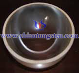 material for microstrip, but its dielectric anisotropy constitutes an important design complication. This paper describes investigations into the quasi-static characteristics of single microstrip lines on sapphire substrates cut with a specified orientation. To account for anisotropy, a new permittivity parameter epsilonreq is introduced, which is a function of the Iinewidth to substrate-height ratio W/h. The variation of epsilonreq with W/h is derived by finite-difference methods. Universal curves for microstrip on correctly orientated sapphire are presented, showing 1) Epsilonreq, 2) The low-frequency limit of effective microstrip permittivity epsilone0, and 3) The characteristic impedance of the line Z0, all as functions of W/h.
A method was developed for depositing silicon films by the pyrolytic decomposition of SiH4 on single crystal sapphire. Electron diffraction and Laue reflection examinations of the films shows single-crystal patterns. The silicon film has a Hall mobility of 135 cm2/volt-second at a hole density of 1017/cm3. Insulated-gate field-effect transistors with a transconductance of 1000 µmho at 5 ma were made with dimensions of 10 µ source-to-drain spacing and an active distance of 120 µ. This value compares favorably with similar units made on bulk silicon and is very encouraging for the possibilities of thin-film silicon devices.
Tungsten Manufacturer & Supplier: Chinatungsten Online - http://www.chinatungsten.com
Tel.: 86 592 5129696; Fax: 86 592 5129797
Email: sales@chinatungsten.com
Tungsten & Molybdenum Information Bank: http://i.chinatungsten.com
Tungsten News & Tungsten Prices, 3G Version: http://3g.chinatungsten.com
Molybdenum News & Molybdenum Price: http://news.molybdenum.com.cn
More Articles...
- High Performance GaN-Based LEDs on Patterned Sapphire Substrate with Patterned Composite SiO2/Al2O3 Passivation Layers And TiO2/Al2O3 DBR Backside Reflector
- 11 PV Industry Company to Profitability
- Three Gorges Group Chengde Photovoltaic Power Plant Commissioned
- Shanxi Accelerate The Healthy Development of The PV Industry



 sales@chinatungsten.com