TDE-Lighttech Releases LED-pixel Module System
- Details
- Category: Tungsten & Sapphire Growth Furnace News
- Published on Friday, 21 February 2014 11:12
- Hits: 2401
The PixLED - RGBW4506 is a LED-pixel module. It is a solid state design equipped with six high intense RGB  LED’s. Due to its ultra-high visual refresh rate (patented technology), the LED-module is extremely suitable for studio and entertainment applications. The PixLED has a true 16 bit colour depth in order to create finer levels of colour and display better gradient effects.
The dome of the is 50mm in diameter and is available in an opal or clear PC lens. The PixLED-modules are daisy chain connected to each other using automatic addressing mode. Each string of PixLED-modules is connected to the AD-UDR1 Dynamic LED-driver with a maximum of 100 modules per driver*
PixLED Features:
- Power : 24VDC
- Consumption : 1,5 Watt / Pixel
- LED’s : 6 x One Chip RGB
- Optics : Opal or Clear dome, 50mm
- String : Maximum 100 x PixLED module*
- Dimensions : ø45mm
*depending on cable lengths and power supply.
Tungsten Manufacturer & Supplier: Chinatungsten Online - http://www.chinatungsten.com
Tel.: 86 592 5129696; Fax: 86 592 5129797
Email: sales@chinatungsten.com
Tungsten & Molybdenum Information Bank: http://i.chinatungsten.com
Tungsten News & Tungsten Prices, 3G Version: http://3g.chinatungsten.com
Molybdenum News & Molybdenum Price: http://news.molybdenum.com.cn
Obstacles And Benefits of Large-Diameter-Based LED
- Details
- Category: Tungsten & Sapphire Growth Furnace News
- Published on Thursday, 20 February 2014 11:48
- Hits: 2473
In summary, we found a move to large-diameter-based LED manufacturing provides a 55% increase in LED 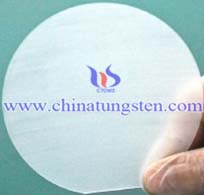 chips per MOCVD run using 6-in wafers, and a 77% using 8-in wafers. In addition to more chips, the yield would increase throughout the manufacturing process due to better epitaxy yield, automation, and process control.
The reason these advantages haven’t become common except with the largest LED manufacturers are several market and technology barriers. These include a-axis sapphire growth technology, a depressed market, and the use of PSS. But new c-axis-growth technology provides an optimized path to supplying large-diameter sapphire substrates. Other substrate materials, such as silicon, will likely find niche uses with some manufacturers.
Large diameter has already been proven by large tier-1 manufacturers as an important component in reducing costs and increasing performance of HB-LEDs. See “Philips Lumileds announces workhorse Luxeon T LED family” (www.ledsmagazine.com/news/9/12/7) for an example.
Yet many companies are staying with small diameter wafers until the next demand wave comes. However, companies that are planning ahead to gain a competitive edge – as is possible with large-diameter LED manufacturing – will be more efficient, more flexible to meet demand, and find success in the future.
Tungsten Manufacturer & Supplier: Chinatungsten Online - http://www.chinatungsten.com
Tel.: 86 592 5129696; Fax: 86 592 5129797
Email: sales@chinatungsten.com
Tungsten & Molybdenum Information Bank: http://i.chinatungsten.com
Tungsten News & Tungsten Prices, 3G Version: http://3g.chinatungsten.com
Molybdenum News & Molybdenum Price: http://news.molybdenum.com.cn
Potential Sapphire Substrate Disruptions
- Details
- Category: Tungsten & Sapphire Growth Furnace News
- Published on Wednesday, 19 February 2014 17:58
- Hits: 2329
It is certain that HB-LED manufacturing will ultimately move to large-diameter sapphire substrates. The 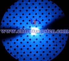 question is how quickly, and what material will be used for the substrates? In this last section we’ll briefly look at potential answers to these questions.
As we said at the beginning, adoption of large-diameter is currently low and predicted to take years to complete. However, advances in alternative substrates to traditional sapphire may accelerate this adoption or carve out niche channels for some companies. But first we’ll focus on sapphire.
The main challenges we noted were the low material utilization due to a-axis growth and the high level of defects that make larger wafers expensive. There are alternative growth technologies that can grow directly on the c-axis for much lower waste. In addition, growth technologies that avoid significant defects are also available.
Sapphire grown with these characteristics of c-axis growth (also called on-axis growth for LED applications) and low defect levels are very well optimized for large-diameter applications.Depicting c-axis CHES technology, the problems of low material utilization and high defect levels are both solved at once, with the additional benefit of a near net shape boule. The result is over 75% utilization for both 6- and 8-in applications.
In addition, the problems of warp during epitaxy that we saw from a-axis-grown sapphire are reduced as the c-axis CHES wafers are grown with a single time signature across their surface (Fig. 8). Because of these advantages, it is expected that as more manufacturers move to large-diameter applications, the growth technologies will also transition to c-axis, low-defect-level growth.
Alternative substrates to sapphire, such as silicon, silicon carbide, and gallium nitride (GaN) are also being researched. A small number of LED manufacturers are even in production on each of these substrates, yet not as a cost-effective alternative to sapphire. Each of these alternatives has certain advantages over sapphire, yet multiple breakthroughs are needed for one of them to significantly displace sapphire. Of the alternative substrates, current predictions give silicon the best chance for success.
Because LEDs have such a broad potential market, there will be room for these alternative substrates along with sapphire remaining predominant. For example, an advantage GaN substrate brings is higher performance per chip – albeit at very high cost. This substrate may find a niche where a single bright LED chip is desired or required.
The next diameter past 6-in is the 8-in wafer. These wafers give another dramatic gain in LED chip count and further opportunities for yield improvement. Yet the barriers we examined earlier are the same, with the addition of the sapphire substrate costs doubling over 6-in using a-axis growth methods. Therefore the prediction is that one of these alternative technologies (sapphire grown on c-axis, silicon, or another substrate) will become dominant for 8-in wafers and beyond.
Tungsten Manufacturer & Supplier: Chinatungsten Online - http://www.chinatungsten.com
Tel.: 86 592 5129696; Fax: 86 592 5129797
Email: sales@chinatungsten.com
Tungsten & Molybdenum Information Bank: http://i.chinatungsten.com
Tungsten News & Tungsten Prices, 3G Version: http://3g.chinatungsten.com
Molybdenum News & Molybdenum Price: http://news.molybdenum.com.cn
LED Market Lightens Up Sapphire Wafer Prospects
- Details
- Category: Tungsten & Sapphire Growth Furnace News
- Published on Thursday, 20 February 2014 11:34
- Hits: 2550
The sapphire wafer market has undergone a downturn in recent quarters, but future prospects are looking  bright based on LED lighting growth. One of the top global sapphire suppliers, Rubicon Technology Inc., based in Illinois, which makes crystalline sapphire substrates and products for the LED, RF-IC, semiconductor and optical industries, reported Q3 revenue of $10.6M on Monday, down 38 percent on $17M year-on-year, but up 28 percent versus $8.3M last quarter. Rubicon announced that the short-term rise in revenue was due to 2- and 4-inch core products increasing from $1M to $6M. However, this rise was partly offset by revenue for 6-inch sapphire wafers falling about 50 percent from $6.1M in Q1 to $3.2M, mainly due to a temporary slowdown in the 6-inch sapphire-on-silicon (SoS) market associated with high inventory levels for RF products in various communications and mobile device applications. The overall revenue growth compared to earlier this year was elevated by the improving LED general lighting market. Furthermore, the slowdown in 6-inch sapphire wafer is stagnating across-the-board factory utilization rates for its various services, contributing to overall revenue losses. On the bright side, a recent market research report has indicated this trend will be reversed.
Displaybank released a report earlier this month on the cost-competiveness of LED chips. According to the report, it will be more profitable for LED chips to be fabricated on higher-price, larger, 6-inch sapphire substrates versus 4-inch by as early as 2015 due to favorable economic and supply chain conditions. In 2012, the 4-inch sapphire ingot/substrate lost its price premium compared to the 2-inch product, and the 6-inch product had to lower its margin because of excess supply in 2013. However, large price fluctuations of this nature are not expected to occur after 2014. What’s more, LED manufacturers are expected to convert their production lines over to 6-inch or 8-inch substrates in the next year amid the falling prices of 6-inch sapphire substrates and enhanced yield rates.
The Displaybank report conducts a thorough analysis on the supply price history, trends and forecast of raw materials associated with packaged LEDs across the entire LED value chain. The key materials include: sapphire ingot, substrate, LED chip, frame packaging (PCB, lead frame, ceramic), phosphor (YAG, silicate, nitride) for color filtering and encapsulation from air contamination. The report compares the production cost and selling price of packaged LEDs by application, analyzes the margin and cost structure, and forecasts for the cost and price over the next seven years. However, it is very difficult to project the LED lighting market out more than three to five years amid the quickly changing dynamics of the industry, which has outperformed most past estimates.
Besides the primary gallium nitride (GaN)-based LED lighting market strategy of fabricating them on sapphire substrates, there are several companies developing technology using the GaN-on-silicon wafer approach due to its lower inherent cost associated with cheaper silicon substrates. Azzurro Semiconductors, headquartered in Dresden, Germany, has helped take GaN-on-silicon epitaxy to the next level, which also includes power control and high-frequency device applications. This company formed a new business unit on Monday to facilitate its patent licensing capability in this regard. Azzurro’s new strategy is to license technology to LED companies globally, as opposed to focusing on manufacturing products like most of the industry. The company has already used its template wafers to quickly streamline the conversion process for customers from GaN-on-sapphire to GaN-on-Si layers. However, a recent study by Lux Research predicted that upstart GaN-on-Si LEDs will only grow to 10 percent of the market by 2020, as sapphire will continue to reign the as king substrate material.
When it comes to patents and IP licensing, there is a true top dog across the high-tech realm. The leading IP development company is InterDigital, which is subsequently the most profitable company in the US, with a net income of $937,255 per worker, according to Bloomberg’s just-released visual compendium of data. This company does not like to be referred to as a patent troll, but the name has stuck due to their immense revenues generated from lawsuits annually. Similar to the top chip design firm, ARM, based in the UK, which dominates the market for processor chips in mobile devices, InterDigital does not manufacture any products; but rather directs its 200 or so engineers to generate IP, often related to microelectronics and communications, that is estimated to be worth billions of US dollars.
Tungsten Manufacturer & Supplier: Chinatungsten Online - http://www.chinatungsten.com
Tel.: 86 592 5129696; Fax: 86 592 5129797
Email: sales@chinatungsten.com
Tungsten & Molybdenum Information Bank: http://i.chinatungsten.com
Tungsten News & Tungsten Prices, 3G Version: http://3g.chinatungsten.com
Molybdenum News & Molybdenum Price: http://news.molybdenum.com.cn
Technology Barriers on Large Diameter Sapphire Substrates
- Details
- Category: Tungsten & Sapphire Growth Furnace News
- Published on Wednesday, 19 February 2014 17:45
- Hits: 2531
The second barrier to the adoption of large diameter sapphire substrates is a group of technological hurdles. It  begins with challenges in sapphire crystal growth–the first step in creating sapphire substrates.Today’s sapphire for HB-LEDs is typically grown on the a-axis, even though HB-LEDs require c-axis wafers. To get c-axis wafers from a-axis sapphire boules, a core must be taken sideways – wasting a large part of the sapphire.
Today’s a-axis sapphire growth technologies also result in defects that cannot be avoided when coring for large diameter applications. The volume of a 6- or 8-in core is so large that the defects become unavoidable and the cores must be shortened or scrapped. The total losses from sideways coring and defects waste over 80% of the material. For 8-in applications, the waste is over 90% and the production costs double.
Another barrier caused by a-axis growth is that the resulting wafers have a variation in stress and strain across their surface. Because the wafer is from a sideways core of the boule, and the boule is grown along the a-axis, the wafer itself has a long growth time signature across its surface. This becomes significant during epitaxial growth when the wafer is heated.
As you can see in the Fig. 6, the wafer will bow in an uneven pattern or a warp. This warping is very difficult to counteract by the MOCVD engineer and has caused several attempted workarounds, including a move to thicker wafers and the use of stress-relieving layers. These techniques add to the production cost and complexity. Without counteracting the warp, the result during epitaxy is lower LED chip yield.
The last technology barrier is in the slicing and polishing of the wafer and application of PSS techniques. Slicing and polishing are difficult processes and must be done well to generate good yield during epitaxy. Because the large wafers are 9-16× larger, the difficulty increases significantly.
PSS application faces a similar challenge, with the additional obstacle that the pattern can only be seamlessly applied to a limited size area smaller than 6 in. In order to get PSS on a 6-in wafer, a stepper (a semiconductor manufacturing tool) must apply multiple patterns, which is common in the silicon industry. However, for HB-LEDs the edges of the multiple pattern applications must be closely matched or LED yield will drop. This accuracy requirement is proving to be very challenging.
These barriers of market conditions and technology challenges have created multiple limitations for the mass adoption of large-diameter substrates. In the future, the market demand will require the throughput and yield only available using larger substrates, and as a result the technology challenges will be overcome. As proof of the possibility of overcoming the challenges, several tier-1 manufacturers have already made the switch and are positioned with an advantage over the majority of the industry.
Tungsten Manufacturer & Supplier: Chinatungsten Online - http://www.chinatungsten.com
Tel.: 86 592 5129696; Fax: 86 592 5129797
Email: sales@chinatungsten.com
Tungsten & Molybdenum Information Bank: http://i.chinatungsten.com
Tungsten News & Tungsten Prices, 3G Version: http://3g.chinatungsten.com
Molybdenum News & Molybdenum Price: http://news.molybdenum.com.cn



 sales@chinatungsten.com