Fabrication of WS2 Nanotubes
- Details
- Category: Tungsten Information
- Published on Saturday, 05 November 2022 22:27
Chemically grown multi-walled WS2 nanotubes are dispersed on SiO2/Si++ substrates. Isolated nanotubes were selected under an optical microscope. single crystals of WS2 were grown by chemical vapor transport. Bilayers and monolayers were mechanically peeled using tape.
Subsequently, these flakes were transferred to a SiO2/Si++ substrate. Their number of layers was determined by contrast in optical micrographs. The electrodes were patterned using electron beam lithography with poly (methyl methacrylate) (PMMA) as resist. After PMMA development, chromium (5 nm) and gold (200 nm) were deposited as electrodes by evaporation.

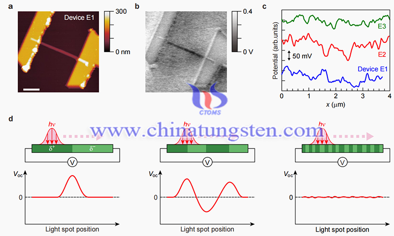
Photovoltaic response measurements. All electrical measurements were performed under high vacuum conditions in an optical thermostat retrofitted with an electrical penetration device. Samples were irradiated by either a He-Ne laser (wavelength 632.8 nm) or one of two diode lasers (532 nm or 730 nm), and the size of the laser spot, determined by a Gaussian fit to the laser profile, was approximately 2.5 µm (632.8 nm), 2.1 µm (532 nm) or 1.2 µm (730 nm).
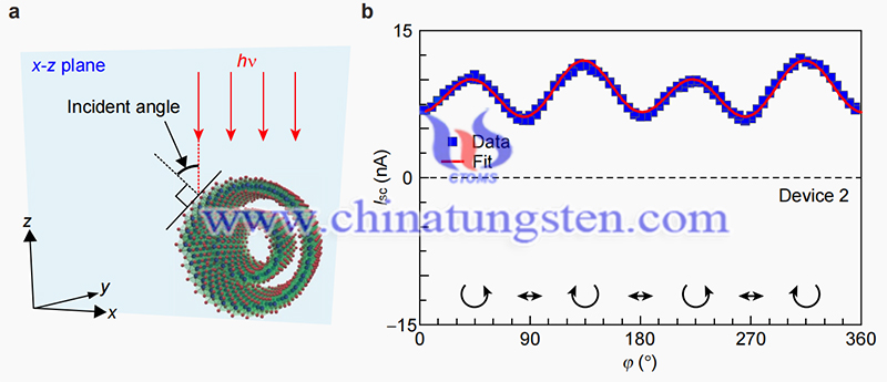
The laser beam is focused on the sample at a normal angle of incidence through an Olympus objective lens of ×50. The tight focus of the laser beam does not affect the quality of the experimental results. The incident laser power was monitored with a power meter located behind the objective lens. The polarization characteristics were modulated by combining a Glan-Taylor prism, a λ/2 plate, and a λ/4 plate.
In WS2 nanotubes, BPVE is several orders of magnitude larger than in other bulk materials. The researchers note that the diameter of the tube (about 102 nm) is much smaller than the diameter of the laser spot (1-2 µm); therefore, the nanotube can absorb at most 10% of the total incident laser power.
The observation of a large BPVE, the first time such an effect has been observed outside the field of bulk materials, shows the potential of TMD nanotubes to harvest solar energy.

Furthermore, the large difference (several orders of magnitude) in effect strength between monolayers (non-polar non-centrosymmetric structures) and nanotubes (polar non-centrosymmetric structures) suggests that reduced symmetry, and perhaps polar crystal structures, are essential for improving BPVE.
Cited paper: Zhang Y J, Ideue T, Onga M, et al. Enhanced intrinsic photovoltaic effect in tungsten disulfide nanotubes[J]. Nature, 2019, 570(7761): 349-353.
- Tungsten Manufacturer & Supplier, Chinatungsten Online: www.chinatungsten.com
- Tungsten News & Prices of China Tungsten Industry Association: www.ctia.com.cn
- Molybdenum News & Price: news.molybdenum.com.cn
- Tel.: 86 592 5129696; Fax: 86 592 5129797; Email: sales@chinatungsten.com


 sales@chinatungsten.com