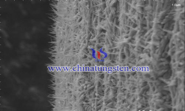
Core-shell Tungsten Oxide Copper Oxide Heterojunction Nanowires
- Details
- Category: Tungsten Information
- Published on Saturday, 09 November 2019 23:11
Nano materials show a series of unique properties in micro scale, such as surface effect, quantum effect, small size effect, quantum tunneling effect and so on. Under the influence of these properties, nano materials, especially one-dimensional nano materials, show outstanding specific surface area, adsorption and desorption performance, which contributes to the development of one-dimensional materials.

At present, the market is mainly through the modification of gas sensing materials to improve gas sensing performance. It can be modified by constructing heterogeneous structure. The application of heterojunction in the field of gas sensing to form heterojunction gas sensing materials is another potential direction to improve gas sensing performance. A core-shell tungsten oxide copper oxide heterojunction nanowire array has been proposed:
Step 1: deposit the tungsten thin film material layer: place the single crystal silicon in the vacuum chamber of the ultra-high vacuum target magnetron sputtering equipment, take the metal tungsten as the target, take the inert gas as the sputtering gas, and deposit the tungsten thin film source material layer on its surface, wherein the inert gas flow rate is 20-55sccm, the sputtering working pressure is 1.0-2.0pa, the sputtering power is 70-110w, the sputtering time is 8-25min, and the gas is argon, helium or nitrogen.
Step 2, crystal growth of one-dimensional tungsten oxide nanowires: the tungsten film prepared in step 1 is placed in a vacuum high-temperature tubular furnace for recrystallization heat treatment. Argon is used as the working gas and oxygen is used as the reaction gas. During the growth process of tungsten oxide nanowires, the flow of oxygen and argon are controlled to be 0.1-0.9sccm and 30-45sccm respectively, and the growth pressure in the furnace is controlled to be 120-250pa. The tube furnace is driven from the room temperature rises from 20-25 ℃ to 600-700 ℃, the heating rate is 3-5 ℃ / min, the temperature is kept at 600-700 ℃ for 1-2 hours, then the temperature drops for 1 hour to 400 ℃, and finally the temperature is naturally cooled to 20-25 ℃.
Step 3, annealing treatment of one-dimensional tungsten oxide nanowire: the one-dimensional tungsten oxide nanowire structure prepared in step 2 was annealed for 1-2 hours under 300-400 ℃ air environment in muffle furnace to further stabilize the crystal orientation.
Step 4: the annealed tungsten oxide nanowires are coated with copper: a copper film is deposited on the substrate of the one-dimensional tungsten oxide nanowires treated in step 3 by ultra-high vacuum magnetron sputtering. The metal copper is used as the target, the inert gas is used as the sputtering gas, the inert gas is argon, helium or nitrogen, the inert gas flow rate is 30-50sccm, the sputtering working pressure is 1.0-2.0pa, and the sputtering work is 1.0-2.0pa. The sputtering time is 0.5-6min.
Step 5, annealing heat treatment of copper: the substrate prepared in step 4 can be annealed for 1-5 hours under 250-500 ℃ air environment in muffle furnace.
Tungsten oxide copper oxide heterostructures form a one-dimensional nanowire array with uniform morphology and structure, which has high specific surface area and excellent heterojunction performance. The special band structure formed by heterojunction can accelerate the electron hole transport rate, provide the sensitivity of gas reaction, and its large specific surface area can contact with gas to improve its response speed. The structure of the heterojunction combined with the one-dimensional nanowire array will have great research space in reducing the working temperature of the sensor, improving the sensitivity and response speed of the sensor.
- Tungsten Oxide Manufacturer & Supplier, Chinatungsten Online: www.tungsten-oxide.com
- Tungsten News & Prices of China Tungsten Industry Association: www.ctia.com.cn
- Molybdenum News & Price: news.molybdenum.com.cn
- Tel.: 86 592 5129696; Fax: 86 592 5129797; Email: sales@chinatungsten.com


 sales@chinatungsten.com