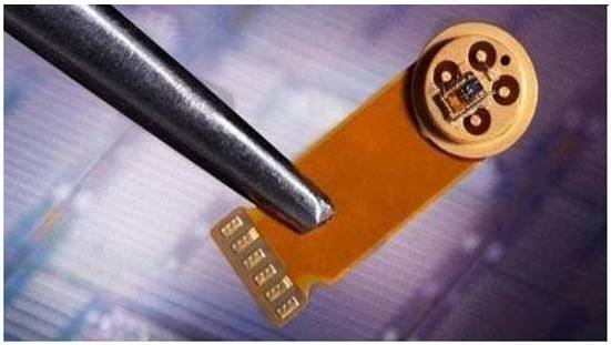
Tungsten Diselenide Thin Film - Indium Oxide Nanowire Composite Near Infrared Photodetector
- Details
- Category: Tungsten Information
- Published on Sunday, 25 August 2019 10:01
The traditional narrow band gap semiconductor is usually used as photosensitive material in infrared detectors. In order to improve the detection sensitivity, shorten the response time of devices and reduce the influence of background noise, the normal operation of these devices requires liquid nitrogen refrigeration environment, which greatly limits the application and working time of devices.

Compared with traditional optoelectronic materials, low-dimensional materials show unique advantages in some semiconductor properties, but the thinner atomic layer thickness of low-dimensional materials also makes it impossible to achieve complete absorption like bulk materials when interacting with light. Therefore, the utilization efficiency of light is low, thereby suppressing the light response rate and detection rate of the device.
In order to overcome the deficiencies of the prior art, the researchers prepared a tungsten selenide thin film-indium oxide nanowire composite near-infrared photodetector, and the preparation process thereof includes:
(1)In2O3 nanowires were grown by chemical vapor deposition.
(2)The In2O3 nanowires prepared in step (1) were physically transferred to a Si/SiO2 substrate.
(3)Single In2O3 nanowires backgate transistors were fabricated by electron beam lithography and hot-evaporation metal electrodes.
(4)WSe2 nanosheets were prepared on another Si/SiO2 substrate by mechanical peeling.
(5)The WSe2 nanosheets prepared in step (4) were transferred to the back-gate transistor devices of In2O3 nanowires prepared in step (3) to obtain the composite structure of tungsten selenide thin sheets and indium oxide nanowires.
Tungsten selenide thin sheet-indium oxide nanowire composite structure can separate the photosensitive material from the conductive channel. It is used to absorb near infrared light. Wide band gap conductive material can obtain very low dark current under gate voltage regulation. At the same time, through the band matching design between the two materials, the energy band at the interface is bent and the photogenerated carriers are in the interface. Local electric field formed by surface accumulation regulates channel conductance and achieves high response and high detection rate.
- Tungsten Oxide Manufacturer & Supplier, Chinatungsten Online: www.tungsten-oxide.com
- Tungsten News & Prices of China Tungsten Industry Association: www.ctia.com.cn
- Molybdenum News & Price: news.molybdenum.com.cn
- Tel.: 86 592 5129696; Fax: 86 592 5129797; Email: sales@chinatungsten.com


 sales@chinatungsten.com