Tungsten Crucible Made Sapphire Wafers - Fingerprint Identification
- Details
- Category: Tungsten's News

| Tungsten Supplier: Chinatungsten Online www.chinatungsten.com | Tel.: 86 592 5129696; Fax: 86 592 5129797;Email:sales@chinatungsten.com |
| Tungsten News & Prices, 3G Version: http://3g.chinatungsten.com | Molybdenum News & Molybdenum Price: http://news.molybdenum.com.cn |
Ammonium Metatungstate(AMT) Industry China Market Research Report 2016
- Details
- Category: Tungsten's News
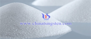
The China Ammonium Metatungstate(AMT) Industry 2016 Market Research Report is a professional and in-depth study on the current state of the Ammonium Metatungstate(AMT) industry.
Russia Plans to Carry Out a Test for Destroying Asteroid by Nuclear Bomb
- Details
- Category: Tungsten's News
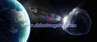

Recently, according to foreign media reports, Russia wants to carry out a nuclear bomb upgrade plan, namely that to emission the nuclear bomb outside of the atmosphere through the intercontinental ballistic missile, in order to destroy asteroids, which would pose a threat to earth.
King of New Materials - Graphene Will Subvert the Future Battlefield, China to Build a Pilot Industry
- Details
- Category: Tungsten's News
Britain has developed a new technology on rapidly mass production; and Chinese experts successfully developed industrial prospect broad Graphene super battery. The Ministry of industry, national development and Reform Commission and the Ministry of science issued Number Opinions on Accelerating Graphene Industry Innovation and Development. Graphene not only has a broad application prospects in the future, but also will bring disruptive change in the future battlefield.

Some scholars said: "nineteenth Century is Iron Age, twentieth Century is Silicon Age, and Twenty-one century is Carbon Age." And Graphene is a representative material of carbon Age. Graphene is stripped out from graphite material, composed of carbon atoms of only one atomic layer, a two-dimensional carbon films with hexagonal honeycomb lattice (benzene). Graphene is a hard material with magic properties of high transmittance, low energy loss. Although graphene has not yet been put into mass production stage, but its excellent performance makes people be full of expectations on the application of future battlefield.
In addition, Graphene is almost zero penetration for gas, liquid and so on. That means coating the ship with Graphene equals to wear a suit of armor "invulnerability". These amazing features also allow Graphene becoming recognized as the king of new materials in just a few decades.
According to opinions, in the future, Graphene will have broad applications on aerospace, weapons and equipment, major infrastructure, and new energy, new energy automotive, energy saving and environmental protection, electronic information and other fields.
| APT Supplier: Chinatungsten Online ammonium-paratungstate.com | Tel.: 86 592 5129696; Fax: 86 592 5129797;Email:sales@chinatungsten.com |
| Tungsten News&Tungsten Prices, 3G Version: http://3g.chinatungsten.com | Molybdenum News & Molybdenum Price: http://news.molybdenum.com.cn |
The United States Worrying China to Sell Semiconductor Equipment at Cabbage Price and Rejected China Takeover of Philps
- Details
- Category: Tungsten's News
On February 5,New York Times publishedAmerican worrying about Chinese ambition in chip is daily increasing, the article said," China is investing heavily to build the domestic semiconductor industry, the upgrade its military forces and local technology industry's move caused by Washington's attention ". In late January 2016, the U.S. foreign investment committee rejected the Chinese investors take over PHILPS's lighting business at 2 billion 900 million, which is a concrete manifestation of the U.S. government concerns.
So, why the United States obstructed the acquisition? The United States government to stop is not the lighting business itself, but to prevent Chinese investors master the technology of the third generation semiconductor materials—GaN, through the acquisition of Philips’s lighting business. LED of GaN has the smaller appearance, higher power and luminosity than the traditional LED; more critical, the density power of GaN is 10 times of the existing GaAs, which can not only widely be used in communication base station, motor vehicles, electric vehicles, wind power and other civilian areas, but also used in the special fields of phased array radar, and make it became a hotspot and frontier of global semiconductor research.
The reason why U.S government stops Chinese investors’ acquisition of Philips’s lighting business is not just for the considering of technology in military applications and national security, but also for restrains the development of China's semiconductor industry, keep its advantage in technology technical.
In short, China support of the local development of the semiconductor industry in the from of semiconductor, IC design, manufacturing, packaging and testing, semiconductor manufacturing equipment, a full range of support, and strive to achieve a "winner" in the form of the whole industry chain. Once the semiconductor industry captured by China, and output the products at "cabbage price", it can weaken American global supremacy material basis on the one hand; on the other hand, it will make China completely get rid of controlled by others in the field of information technology and the harmful situation of information security, presumably this is what Americans really worries.
| APT Supplier: Chinatungsten Online ammonium-paratungstate.com | Tel.: 86 592 5129696; Fax: 86 592 5129797;Email:sales@chinatungsten.com |
| Tungsten News&Tungsten Prices, 3G Version: http://3g.chinatungsten.com | Molybdenum News & Molybdenum Price: http://news.molybdenum.com.cn |
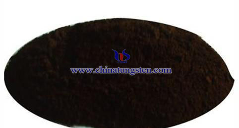
Tungsten Diselenide is Expected to as Thin Flexible Solar Cells
- Details
- Category: Tungsten's News
| Tungsten Supplier: Chinatungsten Online www.chinatungsten.com | Tel.: 86 592 5129696; Fax: 86 592 5129797;Email:sales@chinatungsten.com |
| Tungsten News & Prices, 3G Version: http://3g.chinatungsten.com | Molybdenum News & Molybdenum Price: http://news.molybdenum.com.cn |
Tungsten Diselenide has been Developed as New Flexible Solar Cell Materials in Austria
- Details
- Category: Tungsten's News
| Tungsten Supplier: Chinatungsten Online www.chinatungsten.com | Tel.: 86 592 5129696; Fax: 86 592 5129797;Email:sales@chinatungsten.com |
| Tungsten News & Prices, 3G Version: http://3g.chinatungsten.com | Molybdenum News & Molybdenum Price: http://news.molybdenum.com.cn |
Physical Properties of WTe2 under High Pressure and Strong Magnetic Field II
- Details
- Category: Tungsten's News
| Tungsten Supplier: Chinatungsten Online www.chinatungsten.com | Tel.: 86 592 5129696; Fax: 86 592 5129797;Email:sales@chinatungsten.com |
| Tungsten News & Prices, 3G Version: http://3g.chinatungsten.com | Molybdenum News & Molybdenum Price: http://news.molybdenum.com.cn |
Physical Properties of WTe2 under High Pressure and Strong Magnetic Field I
- Details
- Category: Tungsten's News

| Tungsten Supplier: Chinatungsten Online www.chinatungsten.com | Tel.: 86 592 5129696; Fax: 86 592 5129797;Email:sales@chinatungsten.com |
| Tungsten News & Prices, 3G Version: http://3g.chinatungsten.com | Molybdenum News & Molybdenum Price: http://news.molybdenum.com.cn |
Study on Unique Electronic Valleys of Tungsten Disulfide
- Details
- Category: Tungsten's News
| Tungsten Supplier: Chinatungsten Online www.chinatungsten.com | Tel.: 86 592 5129696; Fax: 86 592 5129797;Email:sales@chinatungsten.com |
| Tungsten News & Prices, 3G Version: http://3g.chinatungsten.com | Molybdenum News & Molybdenum Price: http://news.molybdenum.com.cn |


 sales@chinatungsten.com