100 Years of Doped Tungsten WireⅠ- Early Attempts at Metallurgy
- Details
- Category: Tungsten Information
- Published on Wednesday, 13 July 2022 18:47
- Written by Caodan
- Hits: 1419

From a historical perspective, William D. Coolidge's development PM process and tool "for making tungsten ductile" in 1909 marked the beginning of the use of tungsten filaments in the lighting industry. William D. Coolidge's development of the PM process and tools to "make tungsten ductile" in 1909 marked a breakthrough in the use of tungsten filaments in the lighting industry and began the modern industrial era of Powder Metallurgy.
Read more: 100 Years of Doped Tungsten WireⅠ- Early Attempts at Metallurgy
Six Tips for Caring and Clearing Tungsten Rings
- Details
- Category: Tungsten Information
- Published on Thursday, 23 June 2022 22:55
- Written by Caodan
- Hits: 1399
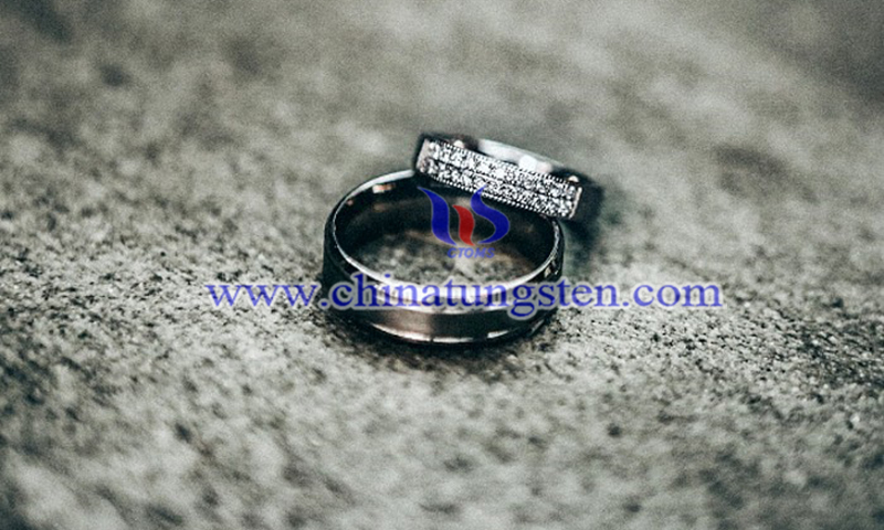
In recent years, tungsten rings have been a popular choice for their durable and scratch-resistant properties. However, they can also lose their luster over time. Below, we will explain how to take care of your tungsten wedding ring.
2D Molybdenum Diselenide and Its Hybrids for Hydrogen Generation Applications
- Details
- Category: Tungsten Information
- Published on Tuesday, 21 June 2022 14:24
- Written by Caodan
- Hits: 1322
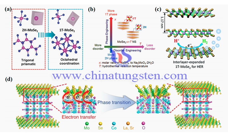
Hydrogen (H2) is a green and economical alternative to conventional fossil fuels due to its zero carbon emission. 2D molybdenum diselenide (MoSe2) hosts significant applications in hydrogen generation due to its low hydrogen adsorption Gibbs free energy and good electrical conductivity. The development of efficient hydrogen evolution reaction (HER) catalysts is of great interest for economical green hydrogen production.
Read more: 2D Molybdenum Diselenide and Its Hybrids for Hydrogen Generation Applications
Atomically MoS2 and WS2 Thin Semiconductors for Nanophotonics
- Details
- Category: Tungsten Information
- Published on Thursday, 23 June 2022 22:47
- Written by Caodan
- Hits: 1251
Atomically thin layers of semiconductors, such as molybdenum disulfide (MoS2) and tungsten disulfide (WS2), are promising materials for nanoscale photonic devices. These nearly two-dimensional semiconductor support so-called excitons or bound electron-hole pairs, which can be aligned vertically along the thin planes of the material.
Read more: Atomically MoS2 and WS2 Thin Semiconductors for Nanophotonics
Properties of Titanium/Tungsten/Graphene Oxide Thin Films
- Details
- Category: Tungsten Information
- Published on Monday, 20 June 2022 23:09
- Written by Caodan
- Hits: 1387
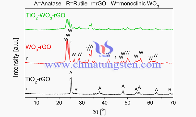
Recent research discusses the optical and self-cleaning properties of composite films titanium/tungsten/graphene oxide thin films. The article, published in Surface and Interface, develops a discussion of the optical properties of photocatalytic titanium dioxide - tungsten trioxide - reduced graphene oxide (TiO2-WO3-rGO) (TWG) and TiO2 films and the feasibility of using these films for different applications, particularly as self-cleaning coatings (SCC).
Read more: Properties of Titanium/Tungsten/Graphene Oxide Thin Films
More Articles...
- Application of Tungsten Grinders in Welding
- Hydrogen-Impurity Induced Magnetism in Molybdenum Ditelluride
- Replacing Lead Oxide with Tungsten Trioxide Improves the Performance of Photovoltaic Front Silver Paste
- Synthesis and Characterization of Molybdenum Carbide Catalysts on Different Carbon Supports



 sales@chinatungsten.com