Advantages of Cut-Resistant Tungsten Wire Protective Gloves
- Details
- Category: Tungsten Information
- Published on Tuesday, 08 April 2025 19:19
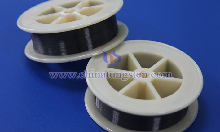
Cut-resistant tungsten wire protective gloves are a kind of hand protection equipment that combines high-strength materials and advanced textile technology. They are widely used in high-risk fields such as industry, manufacturing, and construction. Its core advantages are mainly reflected in the following aspects:
Application of Cut-Resistant Tungsten Wire Protective Gloves
- Details
- Category: Tungsten Information
- Published on Tuesday, 08 April 2025 19:12
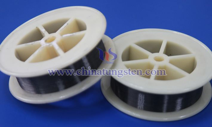
Cut-resistant tungsten wire protective gloves are a high-performance protective equipment, mainly used in scenes where hands need to be protected in high-risk environments. With tungsten wire as the core material and combined with advanced textile technology, this glove has extremely high cut resistance while taking into account flexibility and comfort.
Characteristics of cut-Resistant Tungsten Wire Protective Gloves
- Details
- Category: Tungsten Information
- Published on Tuesday, 08 April 2025 19:09
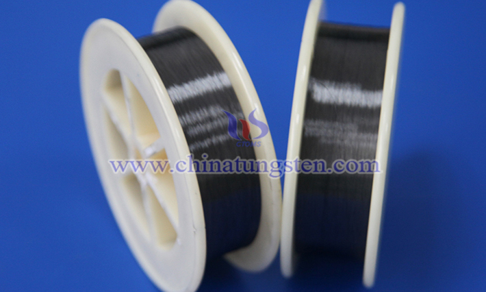
Cut-resistant tungsten wire protective gloves are a specially designed hand safety protection equipment, usually used in scenarios that require high-intensity cut resistance, such as industrial operations, metal processing or glass processing. Its main characteristics include:
Advantages and Disadvantages of Cut-Resistant Tungsten Wire Protective Gloves
- Details
- Category: Tungsten Information
- Published on Tuesday, 08 April 2025 19:08
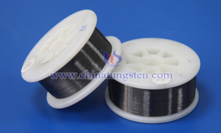
Cut-resistant tungsten wire protective gloves are specially designed protective gloves, usually used in scenarios that require high-strength cut resistance, such as industrial processing, glass manufacturing or metal cutting. The following is an analysis of its advantages and disadvantages:
Performance of Cut-Resistant Tungsten Wire Protective Gloves
- Details
- Category: Tungsten Information
- Published on Tuesday, 08 April 2025 19:02
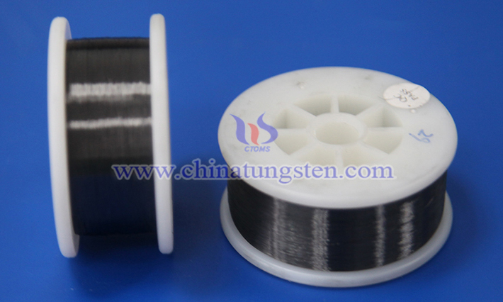
Cut-resistant tungsten wire protective gloves are a type of high-performance protective gear, primarily designed for work environments that require resistance to cutting, piercing, and abrasion risks. Tungsten wire, due to its exceptional strength and durability, is frequently used in manufacturing protective materials that demand superior cut resistance. The main performance characteristics of cut-resistant tungsten wire protective gloves are as follows:
Cut-Resistant Tungsten Wire Protective Gloves
- Details
- Category: Tungsten Information
- Published on Tuesday, 08 April 2025 18:56
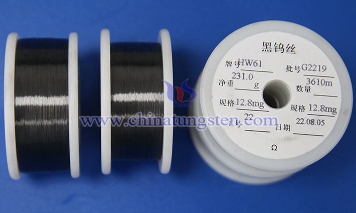
Cut-resistant tungsten wire protective gloves are high-performance protective gear specifically designed for demanding work environments. Utilizing cut-resistant tungsten wire as the core material, these gloves incorporate modern textile technology and blend other high-strength fibers such as high-density polyethylene (HDPE), fiberglass, or nylon to create a product that is both tough and practical.
Protective Clothing Made with Cut-Resistant Tungsten Wire
- Details
- Category: Tungsten Information
- Published on Monday, 07 April 2025 18:44
With the rapid development of modern industry and technology, the importance of protective clothing across various sectors has become increasingly evident. Whether for construction workers, firefighters, or industrial personnel engaged in high-risk operations, protective clothing serves not only as the first line of defense for safety but also as a guardian of life. Among the myriad of protective materials, cut-resistant tungsten wire, with its exceptional properties, is gradually emerging as a favored choice in the field of protective clothing manufacturing.
Cut-Resistant Tungsten Wire for Stone Processing
- Details
- Category: Tungsten Information
- Published on Monday, 07 April 2025 18:42
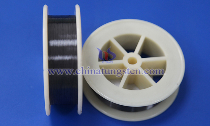
In the modern stone processing industry, efficient, precise, and durable cutting tools are crucial for improving production efficiency and product quality. With continuous technological advancements, cut-resistant tungsten wire has emerged as a high-performance material, gaining prominence in the field of stone processing. Renowned for its exceptional physical properties and chemical stability, tungsten wire has become an ideal choice for cutting hard stone materials. This article explores the characteristics, applications, and significance of cut-resistant tungsten wire in stone processing.
Cut-Resistant Tungsten Wire for Metal Cutting
- Details
- Category: Tungsten Information
- Published on Monday, 07 April 2025 18:39
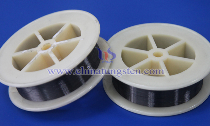
Cut-resistant tungsten wire is a key material in the metal cutting domain. It is widely applied due to its extremely high melting point (approximately 3422°C), exceptional tensile strength, and high-temperature stability, particularly excelling in processing tasks that demand precision and durability.
Cut-Resistant Tungsten Wire for Glass Processing
- Details
- Category: Tungsten Information
- Published on Monday, 07 April 2025 18:37
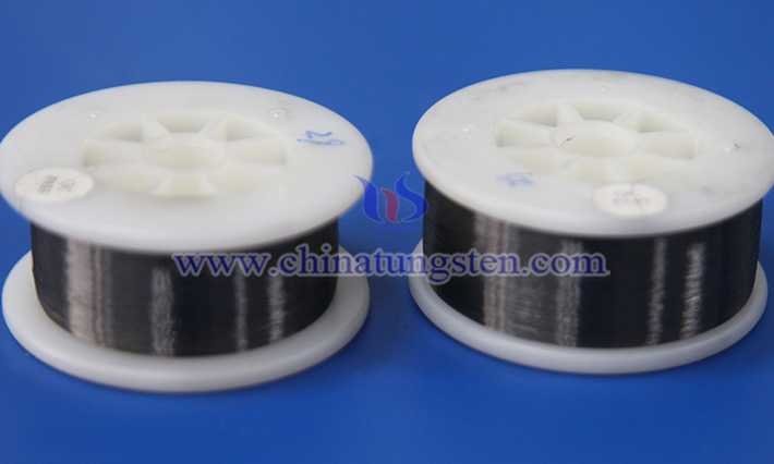
Tungsten (W) is a rare metal with an exceptionally high melting point and hardness. Its unique properties make it an ideal choice for high-precision and high-durability processing tasks. Cut-resistant tungsten wire is a fine, wire-like tool primarily made from tungsten metal. Due to its outstanding physical and chemical properties, it holds a significant position in the field of glass processing.



 sales@chinatungsten.com