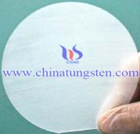
Obstacles And Benefits of Large-Diameter-Based LED
- Details
- Category: Tungsten & Sapphire Growth Furnace News
- Published on Thursday, 20 February 2014 11:48
In summary, we found a move to large-diameter-based LED manufacturing provides a 55% increase in LED  chips per MOCVD run using 6-in wafers, and a 77% using 8-in wafers. In addition to more chips, the yield would increase throughout the manufacturing process due to better epitaxy yield, automation, and process control.
The reason these advantages haven’t become common except with the largest LED manufacturers are several market and technology barriers. These include a-axis sapphire growth technology, a depressed market, and the use of PSS. But new c-axis-growth technology provides an optimized path to supplying large-diameter sapphire substrates. Other substrate materials, such as silicon, will likely find niche uses with some manufacturers.
Large diameter has already been proven by large tier-1 manufacturers as an important component in reducing costs and increasing performance of HB-LEDs. See “Philips Lumileds announces workhorse Luxeon T LED family” (www.ledsmagazine.com/news/9/12/7) for an example.
Yet many companies are staying with small diameter wafers until the next demand wave comes. However, companies that are planning ahead to gain a competitive edge – as is possible with large-diameter LED manufacturing – will be more efficient, more flexible to meet demand, and find success in the future.
Tungsten Manufacturer & Supplier: Chinatungsten Online - http://www.chinatungsten.com
Tel.: 86 592 5129696; Fax: 86 592 5129797
Email: sales@chinatungsten.com
Tungsten & Molybdenum Information Bank: http://i.chinatungsten.com
Tungsten News & Tungsten Prices, 3G Version: http://3g.chinatungsten.com
Molybdenum News & Molybdenum Price: http://news.molybdenum.com.cn


 sales@chinatungsten.com