Wafer-Scalable Single-Layer Amorphous Molybdenum Trioxide
- Details
- Category: Tungsten Information
- Published on Sunday, 06 March 2022 21:00
A research team from the University of Texas at Austin, recently published a study on the use of two-dimensional MoS2 as a starting material to obtain wafer-scalable single-layer amorphous molybdenum trioxide (MoO3).
In this article, the team reports on the precise layer-by-layer conversion of 2D MoS2 crystals to 2D amorphous MoO3 by UV-based ozone conversion, a mild oxidation process suitable for maintaining material integrity. Converting 2-inch polycrystalline monolayers of MoS2 to uniformly continuous amorphous monolayers of MoO3, it can be demonstrated that this conversion method can also be extended to whole wafers.

Molybdenum trioxide, especially α-MoO3, has attracted a great deal of attention due to its thermodynamic stability and layered structure, as well as interesting electronic, optical, catalytic, and electrochemical properties. Notably, α-MoO3 is a semiconductor with large electron affinity, wide bandgap, and high ionization energy. Therefore, many applications, including catalysis, sensors, organic light-emitting diodes (OLEDs), batteries, memories, and electrochromic devices, have been successfully demonstrated by engineering.
Two-dimensional (2D) MoO3 tends to differ in physical and chemical properties compared to its bulk counterparts, and there are many studies on the integration of 2D MoO3 with other 2D materials. Despite the current wealth of physical phenomena and potential technical advantages, material synthesis is not yet mature enough to produce controlled, reproducible growth of large-area, homogeneous, high-quality 2D MoO3 is difficult. Like other 2D materials, the highest quality 2D oxides are usually obtained from the mechanical exfoliation of bulk crystals.
However, this laboratory approach is technically impossible to produce on a large scale due to its random nature, low yield, and inadequate area coverage. Wider area coverage can be obtained by liquid exfoliation. Liquid peeling is an ultrasound-assisted or ion-intercalation-based peeling method that is suitable for producing large-area films. However, poor monolayer yields (no more than a few tens of percent by volume) hinder the translation of research results.

Vapor phase synthesis, particularly physical vapor deposition (PVD), has been known as a scalable and reproducible synthetic method providing well-crystallized films with controlled stoichiometry and morphology. Among the various PVD methods, thermal evaporation has been widely used for the synthesis of α-MoO3 due to the easy control of deposition parameters, and large-area films have been reported in the temperature range of 400-600 °C.
In addition, another vapor phase technique, chemical vapor deposition (CVD), has been successfully applied to the synthesis of MoO3 thin films. In addition, these methods have not achieved precise control of the lateral dimensions and longitudinal thickness of films with uniform atomic layers.
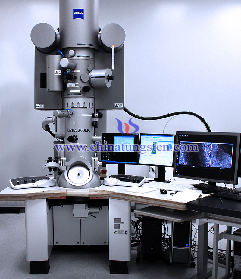
The team has systematically investigated the structural, chemical, optical, and electrical properties of monolayer films by using a combination of spectroscopic and microscopic techniques, including cathodoluminescence (CL) spectroscopy, X-ray photoelectron spectroscopy (XPS), electron energy loss (EL) spectroscopy, scanning transmission electron microscopy (STEM) and atomic force microscopy (AFM).
The team's findings will enable further exploration of sub-nanometer Molybdenum Trioxide, extending the frontiers of ultrathin flexible oxide materials and devices.
| Molybdenum Supplier: Chinatungsten Online www.molybdenum.com.cn | Tel.: 86 592 5129696; Fax: 86 592 5129797;Email:sales@chinatungsten.com |
| Tungsten News & Prices, 3G Version: http://3g.chinatungsten.com | Molybdenum News & Molybdenum Price: http://news.molybdenum.com.cn |


 sales@chinatungsten.com