Waveguide Consists of Tungsten Disulfide Is Thinnest Optical Device Ever!
- Details
- Category: Tungsten's News
- Published on Thursday, 15 August 2019 08:47
Waveguide composed by tungsten disulfide has been developed by the engineers at the University of California San Diego and it is only three layers of atoms thin and is the thinnest optical device in the world! Researchers published their findings on Aug 12 in Nature Nanotechnology.
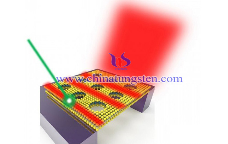
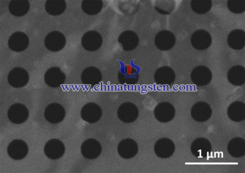
The new waveguide, is about 6 angstroms (1 angstrom = 10-10 meters), 10,000 times thinner than a typical fiber, and about 500 times thinner than an on-chip optical device in an integrated photonic circuit. It consists of a single layer of tungsten disulfide suspended on a silicon frame (a layer of tungsten atoms is sandwiched between two sulfur atoms), and the single-layer forms a photonic crystal from a series of nanopore patterns.
This single layer crystal is special in that it supports electron-hole pairs called excitons, at room temperature, these excitons generate a strong optical response such that the refractive index of the crystal is approximately four times the air refractive index around its surface. In contrast, another material having the same thickness does not have such a high refractive index. As light travels through the crystal, it is captured internally and conducted along the plane by total internal reflection.
The waveguide channels light in the visible spectrum is another special feature. Waveguiding has previously been demonstrated with graphene, which is also atomically thin, but at infrared wavelengths. The team demonstrated for the first time waveguiding in the visible region. Nanosized holes etched into the crystal allow some light to scatter perpendicular to the plane so that it can be observed and probed. This array of holes produces a periodic structure that makes the crystal double as a resonator as well.

This also makes it the thinnest optical resonator for visible light ever to be demonstrated experimentally. This system does not only resonantly enhance the light-matter interaction, but also serves as a second-order grating coupler to couple the light into the optical waveguide.
Researchers used advanced micro- and nanofabrication techniques to create the waveguide. Creating the structure was particularly challenging. The material is atomically thin, so researchers devise a process to suspend it on a silicon frame and pattern it precisely without breaking it.

The tungsten disulfide waveguide is a proof of concept for scaling down the optical device to sizes that are orders of magnitude smaller than today's devices. It could lead to the development of higher density, higher capacity photonic chips.
- Tungsten Manufacturer & Supplier, Chinatungsten Online: www.chinatungsten.com
- Tungsten News & Prices of China Tungsten Industry Association: www.ctia.com.cn
- Molybdenum News & Price: news.molybdenum.com.cn
- Tel.: 86 592 5129696; Fax: 86 592 5129797; Email: sales@chinatungsten.com


 sales@chinatungsten.com