The Story of Solid State Hard Disk and Six Tungsten Chloride
- Details
- Category: Tungsten's News
- Published on Saturday, 02 June 2018 15:37
Today, the China Tungsten online will bring some good news to friends who have not bought solid state hard disk, that is, solid state hard disk is expected to improve quality and price reduction in 2018.

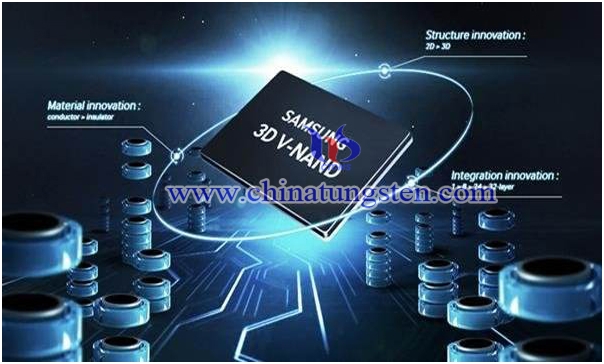
In 2017, Samsung and Toshiba, which monopolized the memory particle market, led to a rise in price fluctuations because of upgrading the 2D NAND flash memory particles, adjusting production lines and reducing production capacity. However, as the new production line has been completed recently, the 2D NAND production line will be upgraded to 3D NAND, and the maximum capacity will be raised to above 2T. When 3D NAND becomes the main force of the market, there will be a great demand for the special gas market, which includes the application of new gases such as six tungsten chloride (WCI6) and sulphur dioxide(SO2).
Six tungsten chloride, also known as tungsten chloride, is an important raw material for new materials. It is a raw material of carbon based on tungsten. Similar to the six tungsten fluoride we know, it will also be used as raw material for metal tungsten chemical vapor deposition (CVD) process in semiconductor production.
Flash memory particles are nonvolatile memory, that is, in the case of power off, it still can save the data that has been written, and is in a fixed block, rather than in a single unit of cell life, cell phone memory, computer memory, solid hard disk, even the U disk is flash memory.
NAND flash memory is a kind of memory particle, which was developed and marketed by Hitachi in 1989. The NAND flash memory particles have many advantages, such as lower power consumption, lower price and better performance, which are mainly used to make solid state hard disks. Due to the recent surge in prices, the supply of memory market will likely become more demanding in the future.
For many years, 2D NAND has been the driving force of semiconductor industry photolithography. However, with the constant approaching of the physical limit of the wafer, the flash memory particles that can be loaded inside the single storage unit on the solid state hard disk are close to the limit, and each unit becomes very small and the single disk capacity is close to the limit.
The concept of 3D NAND is put forward, which is to add another height to the original 2D length and wide space, that is, the memory particles are not only horizontally arranged, but also arranged up, shape growing, wide, high 3D stereoscopic architecture. Using the flash memory particles in the same volume size, the volume of the flash memory particle single disk is greatly improved, and the overall capacity of the storage particles is further enhanced. The height of 3D NAND can be 32, 64, 72 or even 96 layers. The number of layers can be stacked at will, but the volume can not be increased. It is very difficult for many manufacturers, and it will be difficult without technical accumulation.
The 3D NAND process starts from a substrate. Then suppliers begin to experience the first great challenge in the process -- alternately stacked deposits. Using chemical vapor deposition (CVD), alternately stacked deposition involves a process of depositing and stacking thin film layers on a substrate.
This process is more like making a sandwich cake. In short, a material layer is deposited on the substrate, and then a material layer is listed again. This process is repeated several times until the device reaches the desired number of layers. It is said that four or five more processes are needed for each additional layer, and it is estimated that the 64 tier version requires about 300 processing, about 350 of the 72 layer versions and about 450 of the 96 layers. The number of layers is increasing, and design changes are being carried out at the same time to form thinner film and reduce device size. The amount of gas, such as six tungsten chloride (WCI6) and sulfur dioxide (SO2), is increased with the increase of the number of layers, but the thinner film means that the increase is not linear.
This process is not only introduced into 3D-NAND, but also introduced into FinFET and DRAM. It is estimated that the global demand for tungsten chloride six will reach hundreds of tons per year. In terms of capacity, more than 60% of tungsten chloride in the world will be produced in the mainland of China.
Copyright statement: This article is used only for the China Tungsten Industry Association and China Tungsten online. Any individual without written permission or without the copyright and the source is not allowed to copy or reprint without authorization. Otherwise, this website will be regarded as a tort, and the website will be investigated for its legal responsibility.
- Tungsten Manufacturer & Supplier, Chinatungsten Online: www.chinatungsten.com
- Tungsten News & Prices of China Tungsten Industry Association: www.ctia.com.cn
- Molybdenum News & Price: news.molybdenum.com.cn
- Tel.: 86 592 5129696; Fax: 86 592 5129797; Email: sales@chinatungsten.com


 sales@chinatungsten.com