What Is Sapphire Glass
- Details
- Category: Tungsten & Sapphire Growth Furnace News
- Published on Thursday, 15 May 2014 11:01
- Hits: 3138
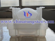
Sapphire glass, except for its cost, has some incredibly desirable qualities. It’s highly transparent between 150nm (ultraviolet) and 5500nm (far-infrared), much stronger than normal glass, and it’s one of the most scratch-resistant materials in the world — it scores 9 on the Mohs scale, one down from diamond’s 10, and quite a lot tougher than Gorilla Glass’s ~7. Its transparency, plus its very high melting temperature (~2,000C) and high thermal conductivity, make it almost uniquely suited for use in arc lamps, laser tubes, and other extreme use-cases. Oh, it’s highly resistant to acids and other caustic substances, too.
In short, it’s an amazing material that’s almost perfectly suited to the front face of the iPhone 6 or iWatch — as long as it can be produced economically. Presumably, with Apple’s recent investment in GT Advanced Technologies, and plans to begin sapphire glass production at a plant in Arizona, the folks in Cupertino believe it’s possible.
Tungsten Manufacturer & Supplier: Chinatungsten Online - http://www.chinatungsten.com
Tel.: 86 592 5129696; Fax: 86 592 5129797
Email: sales@chinatungsten.com
Tungsten & Molybdenum Information Bank: http://i.chinatungsten.com
Tungsten News & Tungsten Prices, 3G Version: http://3g.chinatungsten.com
Molybdenum News & Molybdenum Price: http://news.molybdenum.com.cn
Why Apple Is Investing in Sapphire Glass for The iPhone 6
- Details
- Category: Tungsten & Sapphire Growth Furnace News
- Published on Thursday, 15 May 2014 10:51
- Hits: 3134
It is now fairly clear that Apple is investing heavily in the production and machining of sapphire glass for its future products. Sapphire glass isn’t a new material, but it’s only in recent years, due to improved manufacturing methods, that we’ve started to see it used commercially. The iPhone 5′s camera was protected by a small piece of sapphire glass, and the iPhone 5S’s new home button/fingerprint scanner is made from sapphire glass. Historically, sapphire has been used for the front cover of high-end wristwatches. Now, it seems Apple is preparing to launch an iPhone or iWatch with its entire front face protected by sapphire glass. Why is sapphire glass suddenly so hot? After leading the pack for a few years, has Corning’s Gorilla Glass finally met its match?
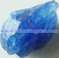
Despite its name, sapphire glass isn’t actually a glass — it’s a single crystal of transparent sapphire. This sapphire is created synthetically, using a similar process to how the semiconductor industry grows single crystals of silicon (the Czochralski process). Basically, a tiny piece of sapphire (a seed crystal) is dipped into a vat of molten alumina (Al2O3), and then slowly drawn upwards, forming very long, carrot-shaped crystals called boules (part of a boule is pictured above). These crystals are then sliced with a saw, and shaped/polished accordingly. (The same method is used to slice silicon wafers from large silicon boules.)
Tungsten Manufacturer & Supplier: Chinatungsten Online - http://www.chinatungsten.com
Tel.: 86 592 5129696; Fax: 86 592 5129797
Email: sales@chinatungsten.com
Tungsten & Molybdenum Information Bank: http://i.chinatungsten.com
Tungsten News & Tungsten Prices, 3G Version: http://3g.chinatungsten.com
Molybdenum News & Molybdenum Price: http://news.molybdenum.com.cn
Simulation and Analysis of GaN Wafer Bowing on Sapphire Substrate
- Details
- Category: Tungsten & Sapphire Growth Furnace News
- Published on Wednesday, 14 May 2014 16:22
- Hits: 3204
During the process of heteroepitaxial growth, if the lattice constant of the growing film differs from that of the substrate, the wafer surface bows, regardless of whether the lattice mismatch occurs or not. As the growth in large-scale wafers speeds up, bowing effects are becoming more and more important. Wafer bowing has a direct impact on the yield in modern mass-production compound semiconductor industries. By using finite element analysis software, the bowing deformation of the GaN wafer on sapphire substrate can be studied. This paper summarizes the causes of bowing deformation, builds the mathematical model, and deduces the relation equation of the wafer bowing. The results show that epitaxial wafer bowing has a linear relationship with the square of the diameter of the substrate but has little relationship with the thickness of the substrate. Moreover, the relation equation of the wafer bowing is also simplified finally.
The MOCVD growth process can be divided into four phases: a reactant input phase, a reactant mixing phase, an immediate boundary layer phase above the substrate, and the growth phase on the substrate surface itself. Growth complications that can occur in these phases include gas phase reactions during reactant mixing, reactant diffusion and/or pyrolysis in the boundary layer above the substrate, and thermodynamic or kinetic rejection of species from the substrate. The worst effects can be reduced or eliminated by providing appropriate equipment design and process conditions.
Tungsten Manufacturer & Supplier: Chinatungsten Online - http://www.chinatungsten.com
Tel.: 86 592 5129696; Fax: 86 592 5129797
Email: sales@chinatungsten.com
Tungsten & Molybdenum Information Bank: http://i.chinatungsten.com
Tungsten News & Tungsten Prices, 3G Version: http://3g.chinatungsten.com
Molybdenum News & Molybdenum Price: http://news.molybdenum.com.cn
Analyzed by MOCVD GaN-Based Optoelectronic Devices Grown on Sapphire Substrates
- Details
- Category: Tungsten & Sapphire Growth Furnace News
- Published on Wednesday, 14 May 2014 16:28
- Hits: 3303
Using MOCVD (metal-organic chemical vapor deposition) to analyze the growth of GaN-base photoelectric  devices on the sapphire substrate is a common method in the semiconductor lighting industry. In recent years, along with the unceasing enhancement of epitaxy technology and related technologies, larger sapphire substrates are needed. The optimization and improvement of MOCVD reaction chamber structure with large-scale epitaxial wafers have been studied by many domestic researchers. Li et al. optimized high-frequency heating graphite base groove structure with eight-inch and twelve-inch substrates. Ying-lu et al.studied the heating modulate curve of radiation heating MOCVD and proposed the design principles of the outer heater. To improve the production efficiency, some great MOCVD manufacturers also focus on how to improve and increase the MOCVD cavity and the sapphire substrate size in foreign countries. At present, two-inch and four-inch epitaxial wafers are frequently used, so manufacturers who can produce six-inch SiC and Si substrate epitaxial wafers with high quality in foreign countries would sell chips abroad.
With the growth of the III-nitrides, sapphire becomes the most extensively used substrate material. Crystals of sapphire with good quality and low price can be easily got. Besides, sapphire is stable at high temperature and the growth technology of nitrides on sapphire is now fairly mature. However, the problem of wafer bowing, which results from the difference in thermal expansion coefficient between GaN epitaxial layer and sapphire, has become much more serious in larger-diameter wafers. It will deteriorate the contact between the substrates and the equipment stages or the subsectors during device process, which will result in degradation in the device uniformity or failures in lithography.
By using finite element simulation software, the relationship between the maximum wafer bowing and sapphire substrate size under characteristic temperature is studied in the case of the growth of GaN in the sapphire substrate, and the wafer bowing relation equation is also deduced. The research work in this paper plays a foreshadowing role for later research sapphire epitaxial growth and MOCVD reaction chamber structure improvement.
Tungsten Manufacturer & Supplier: Chinatungsten Online - http://www.chinatungsten.com
Tel.: 86 592 5129696; Fax: 86 592 5129797
Email: sales@chinatungsten.com
Tungsten & Molybdenum Information Bank: http://i.chinatungsten.com
Tungsten News & Tungsten Prices, 3G Version: http://3g.chinatungsten.com
Molybdenum News & Molybdenum Price: http://news.molybdenum.com.cn
LED Lighting Technology Breakthrough
- Details
- Category: Tungsten & Sapphire Growth Furnace News
- Published on Tuesday, 13 May 2014 11:34
- Hits: 3246
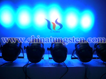
" This year's government work report repeatedly mentioned energy conservation, promote energy production and consumption patterns change, increase energy conservation efforts to control total energy consumption , reduce energy consumption intensity . "CSA production research analyst reports, from March 1, 2014 implementation of the " LED stage lighting General technical conditions "," lighting equipment import and export inspection procedures - Part 2: LED modules for general lighting " , and further refinement of the LED lighting related product standards ; while the previous February 19 , Science and Technology , and the Ministry of industry and Information Technology issued " on the issuance of 2014-2015 energy saving technology special action program " which encourages the semiconductor lighting industry with a clear prospects for significant energy saving technology , through further deepen implementation of the " city of ten thousand ," semiconductor lighting demonstration project engineering and other industries , encourage enterprises to increase investment in research to further expand its market share through technological innovation.
The first quarter record luminous efficiency LED lighting constantly refreshed . In March this year , Cree single white power LED light effect devices exceeded 300 mark, at room temperature to 350MA drive , color temperature 5150K , the luminous efficiency of 303lm / w. This makes the light efficiency contest upgrade again , it also raised the limit for LED luminous efficiency arguments.
CSA production research analyst believes that high light efficiency and high light quality is not an either-or "zero sum game" , through the light efficiency and light quality to enhance the effective integration of optical quality , and promote the healthy development of LED industry is the ultimate goal .
In addition to outside light efficiency , LED lighting products, intelligent heat has repeatedly improved. Many international manufacturers of LED lighting products, systems ISP positive change through intelligent system integration of lighting systems , to further improve lighting energy efficiency and energy conservation. While domestic enterprises also have to enter the field of intelligent lighting , introduced color LED dimmable lamps . According to preliminary estimates CSA production research department , the demand for our intelligent lighting products annually more than 10 million ; addition, China now has "smart city " pilot 193 , the next building and smart home concept combines the wisdom of the city's popular, intelligent lighting with a bright future .
Of course, this quarter , LED lighting creative products are constantly debut. Li Ka-shing 's investment shares which Nanoleaf nanometer semiconductor lighting LED bulbs , and the United States National Key Laboratory of its Order of Grand Goccia company developed the smart button is eye-catching.
Tungsten Manufacturer & Supplier: Chinatungsten Online - http://www.chinatungsten.com
Tel.: 86 592 5129696; Fax: 86 592 5129797
Email: sales@chinatungsten.com
Tungsten & Molybdenum Information Bank: http://i.chinatungsten.com
Tungsten News & Tungsten Prices, 3G Version: http://3g.chinatungsten.com
Molybdenum News & Molybdenum Price: http://news.molybdenum.com.cn


 sales@chinatungsten.com