100 Years of Doped Tungsten Wire Ⅳ- Scientific Background of Doped Tungsten Wires and Outlook
- Details
- Category: Tungsten Information
- Published on Wednesday, 13 July 2022 19:43
Scientific background of doped tungsten wires
The systematic and purposeful doping of tungsten oxide powders was already patented in 1922. However, the doping of elemental potassium and its role in the formation and stabilization of creep-resistant recrystallization intercalated microstructures was only understood after 1964, when new tools for scanning and transmission electron microscopy and new instruments for surface analysis, especially Auger-Electron-Spectrometry (AES), could be used to perform modern microstructural and chemical analysis of nanometer-sized aggregates. Modern microstructural and chemical analyses were performed.
Doped tungsten is unique because it is a "composite" of two unalloyed components, tungsten and potassium. The latter, in minute concentrations in the parts per million (ppm) range, are called dopants and are distributed in the tungsten wire as longitudinally arranged nanoscale bubbles (about 5-50 nm) filled with liquid or gaseous potassium. They interact with all lattice defects, act as dislocations (dislocations) as well as fixation points for dislocation networks (see Figure 13) and act mainly as hindrances to prevent migration of subgrain and grain boundaries. After recrystallization, the bubbles stabilize the creep-resistant overlapping grain structure. Today, potassium bubbles form the strongest known high-temperature barrier. However, at ultra-high temperatures above 3000°C, bubble migration and anomalous grain growth occur due to temperature gradients and the presence of mechanical stresses and impurities, which in turn lead to microstructural instability. So far, tungsten technology is a paradigm because it provides important material science lessons in terms of processing, interactions between microstructure and properties, and material-induced failure mechanisms of lamps.
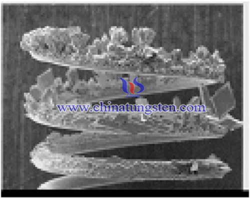
Fig. 12. Tungsten crystal growth in halogen lamps (M=600:1)
Since the discovery of the light bulb in the 1960s, many papers have been published on the light bulb effect of tungsten. The following topics are included.
- The formation of bubble-forming compounds during doping and their incorporation by CVT (chemical vapor transport) processes during reduction.
- The detection of potassium as bubble forming element.
- Evolution of the bubble during the sintering process.
- Deformation during processing.
- Bulb formation engineering from narrow deformed cylinders or ellipsoids.
- Size and growth of the bubbles.
- Observation of the bubble under certain conditions (stress, impurities).
Observed that under certain conditions (stress, impurities), the bubble can grow to extremely large sizes larger than 10 μm in diameter, leading to the failure of high-performance halogen filaments.
Table 2 provides an overview of the important steps in the evolution of knowledge about the light bubble effect.
In general, the following items are agreed in the literature as established facts.
- During the doping process, amorphous and/or crystalline KAlSi3O8, KAlSi2O6 and Al2O3 particles have been formed with sizes between 5 and 50 nm due to the complex chemistry of the W-K-Si-Al-O-NH3 system.
- In the next hydrogen reduction step, these particles will be incorporated into the powder particles by the CVT reaction, leading to the overgrowth process of tungsten particles within the powder bed and the formation of the neck.
- During sintering, the dopant particles decay and silicon and aluminum as well as oxygen are soluble in the tungsten matrix and can diffuse through the open pore channels as well as through the grain boundaries in the second sintering stage. The insoluble potassium forms the bulb, which is stabilized at high temperatures by an equilibrium between the Laplace pressure of the bulb and the internal potassium high-pressure vapor.
- The following thermal deformation steps through rolling, pressing and drawing of sintered ingots, depending on the type of deformation as well as the temperature and speed, cause a significant refinement of the microstructure. The bubbles will be deformed together with the tungsten substrate, corresponding to a change in the overall shape to a narrow ellipsoid or tube.
- In the intermediate annealing stage, the bubble tube spheroidizes into a single bubble or into a row of bubbles, and its behavior is determined by the critical aspect ratio of the bubble tube, which corresponds to the Rayleigh mechanism for the dissolution of a cylindrical fluid into a sphere.
- When bubbles are formed by the dispersion of potassium ellipsoids, they grow to an equilibrium size at elevated temperatures. The equilibrium radius can be expressed exactly by balancing the pressure in the bubble produced by the potassium vapor with the opposite pressure produced by the surface tension of the solid tungsten (Laplace pressure).
- Mechanical stress, temperature gradients and/or impurities can cause abnormal growth of the bubble, resulting in cavities up to 10 microns in diameter and subsequent "hot spots" (cavities that affect resistance, leading to increased evaporation and local thinning of the filament), leading to failure of the tungsten filament.
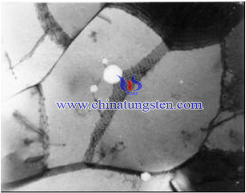
Fig. 13. Interaction of dislocation networks with potassium bubbles (M=56,000:1)
Since 1968, many valuable papers have been published at the Plansee Symposium, especially the 1989 book of “The Metallurgy of Doped/Non-Sag Tungsten” edited by E. Pink and L. Bartha, which provides an excellent compendium of knowledge on the subject.C. L. Briant and B. P. Bewlay give a more recent and short review of the physical and metallurgical background of the Coolidge process.
However, there are still some gaps in scientific knowledge, such as: new requirements in controlling the process steps, new challenges in gaining a deeper understanding of the main material properties and incorporating multi-scale modeling, including the development of corresponding microstructural evolution equations and the adequate characterization of the material properties and their implementation for the prediction of material reactions.
In particular, the following topics:
- Deformation mechanisms during wire processing.
- Dynamic recovery and dynamic recrystallization during deformation.
- High temperature - low stress creep
- Fracture mechanisms, and the transition from ductility to brittleness.
The next two examples illustrate the advances and shortcomings in metallurgical knowledge regarding the microscopic evolution and fracture of the fiber structure during the drawing process. The micrographs presented by TEM and SEM show that the subgrain and grain width neither obey the axisymmetric lengthening corresponding to the wire diameter reduction nor the double-slip plane strain flow during the drawing process (Figure 14). Both predictions fail for true strains greater than 1.5, suggesting a loss of subgrain due to the dynamic recovery process. Recent EBSD investigations have shown that dynamic recrystallization processes are triggered during rolling and forging of tungsten ingots due to a high reduction in deformation temperature and area.
Due to the Hall-Petch effect, the fiber size of heavily drawn tungsten wires, down to about 100 nm, contributes about 33% to the flexural force and tensile strength. This is illustrated in Figure 15a, which shows the rupture of a single fiber after necking down to a chisel edge type with little interference from neighboring fibers. This microstructure combined with the high dislocation density in the range of 2 × 10 15 m-2 could explain the high strength and high ductility of 5.2 GPa, but the mechanisms concerning the relatively independent fiber deformation are not fully understood. In addition, Fig. 15d shows some peculiarities such as cavity growth, trans-crystalline and trans-crystalline fracture, and apparently stable potassium vesicles, which have not been fully explained until now either.
Table 2 Evolution of the knowledge of potassium bubble effects in tungsten

a SANS=Small Angle Neutron Scattering.
Conclusion and outlook
The development of the Coolidge process has had a huge impact on the modern PM industry, especially on the global lighting industry, due to its importance to the requirement of improving the energy efficiency of lamps. To date, the Coolidge process is still the subject of research. Higher energy efficiency means higher requirements for filament temperature and geometric stability. This places more stringent requirements on the performance of the filament, especially the high temperature creep strength, which must be optimized by corresponding thermomechanical processing for proper microstructure formation.
However, despite the progress made in understanding the microstructural evolution of doped tungsten filaments, there are still some questions to be addressed and we have to prepare for further challenges. One of the issues currently debated in the scientific community is whether the bubble rows into which the potassium bubbles are aligned during the thermo-mechanical deformation. Also, the discrepancy between experimental and calculated results regarding the aspect ratio of the potassium bulb ellipsoid caused by deformation needs further justification. Furthermore, the current understanding of the dynamic recovery, recrystallization and grain growth that occur during processing is only preliminary, and the understanding of the mechanisms by which tungsten wires gain high-temperature strength and creep resistance is also at an initial stage. In particular, the bulb growth mechanism is of particular interest due to the impact on the failure mechanism of high-performance halogen lamps.
Furthermore, in order to gain a more comprehensive understanding of the microstructural evolution throughout the production process and the corresponding influence on tungsten properties, it is necessary to combine the modeling efforts of modern atomistic foundations with microstructural observations as well as macroscopic material reactions. A more recent example showing an atomistic model of grain boundary fracture of tungsten is given in Figure 16.
Finally, some concluding remarks on an actual topic of discussion in the community.
“Further substitution and, finally, ban of incandescent lamps”.
Today, about 19% of the global electric power produced worldwide serves for light production from several billion lamps. The majority of this energy is consumed by gas-efficient electric lamps (about 70%), with only a small percentage (about 30%) consumed by incandescent lamps. 80% of the lighting consumer market is professional lighting (industrial, commercial, public), and only 20% is for private consumers.
On March 1, 2007, the European Lamp Companies Federation (ELC) announced an industry commitment to support the government's shift to more efficient lighting products in the domestic market. At the same time, the European Parliament confirmed the roadmap (see Figure 17) and the elimination of the least efficient lamps from the European market by 2015, which is estimated to reduce CO2 emissions by 23 megatons and save approximately 63,000 GWh of electricity per year.
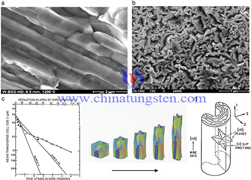
Fig. 14. Longitudinal and transversal fibre morphology of doped tungsten wire (above) fibre with function of true strain, modelling of fibre aspect ratio, slip system and subgrain curling due to plane-strain deformation during wire drawing. Modelling courtesy of J. Ocenasek, Prague, 2005.
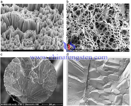
Fig. 15. Fracture morphologies of doped tungsten wires; a) ductile single fibre rupture; b) ductile dimple fracture ,T=1700 °C; c) transcrystalline cleavage with river lines after 1700 °C anneal; d) creep failure with stress induced bubble growth, T=3,200 °C (M=10,000:1)
Over the last three decades, incandescent lamps have been gradually replaced by an increasing number of high-efficiency discharge lamps (CFLs, fluorescent tubes, HP mercury vapor, metal halide, LP sodium or HP sodium, short arc lamps) and IRC- (infrared coated) halogen lamps, among others. However, this evolution of replacement by more efficient light sources has not reduced the consumption of tungsten in lighting, since all these lamps contain tungsten either as coiled filaments or as electrode material in various shapes.
The current discussions about modern lighting, energy conservation, minimizing CO2 emissions and global warming, and subsequent product replacement will not negatively impact tungsten demand in the near future.
Modern 18W - CFL coils (2 times 14 mg), do use the same amount of tungsten as 100W incandescent lamps (28 mg). However, despite the greatly increased lifetime, in the current era, more lights will be needed as more light will be produced. In the long run, the increase in LEDs could have a negative trend, not only in areas such as traffic lights, automotive rear lights, dashboards, and car radios, but also in home lighting. As of today, more tungsten is being used for lighting than ever before due to a still growing global market and the fact that tungsten is being used as a coil and electrode material for most replacement devices.
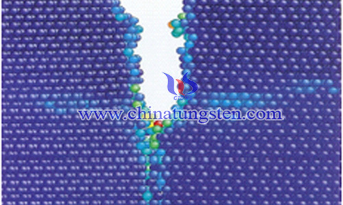
Fig. 16. Atomistic modelling of grain boundary fracture in tungsten.
Courtesy of P. Gumbsch, Freiburg
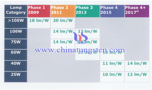
Fig. 17. Replacement scheme of incandescent lamps.
(ELC Background document, Brussels, 2007)
In addition, tungsten is used to a greater extent in high luminous flux applications such as lithography, semiconductor technology, IMAX projection, but also in the environmental industry (water cleaning) and modern laser technology.
(Credit: P. Schade “100years of doped tungsten wire”, International Journal of Refractory Metals and Hard Materials, Volume 28, Issue 6, 2010, Pages 648-660, ISSN 0263-4368)
- Tungsten Manufacturer & Supplier, Chinatungsten Online: www.chinatungsten.com
- Tungsten News & Prices of China Tungsten Industry Association: www.ctia.com.cn
- Molybdenum News & Price: news.molybdenum.com.cn
- Tel.: 86 592 5129696; Fax: 86 592 5129797; Email: sales@chinatungsten.com


 sales@chinatungsten.com