Scientists Have Developed "Nano-Scale Sculpture Technology"
- Details
- Category: Tungsten's News
- Published on Friday, 19 July 2019 17:33
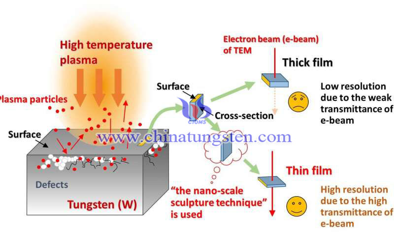
A team of fusion scientists has successfully developed a "nano-scale sculpture technology" to fabricate ultra-thin films by sharpening tungsten samples with focused ion beams. This makes it possible to use transmission electron microscopy (TEM) to observe cross sections very close to the top of tungsten samples at nano-scale. The sculpture technology developed in this study is applicable not only to tungsten, but also to other hard materials.

Hardening materials such as metals, carbon and ceramics are used in automobiles, aircraft and buildings. In the research of fusion reactor, tungsten, as one of the hardest metal materials, is most likely to be the armor material for receiving plasma thermal/particle loads. The device is called a diverter. In any hardened material, nano-scale damage or defects can be formed near the top surface of the material. In order to predict material life, it is necessary to understand the damage types and depth profiles in materials. For this reason, we must observe the cross section of the area very close to the top surface of nano-materials.
In order to observe the internal structure of nano-scale materials, transmission electron microscopy (TEM), which accelerates the transmission of electrons through target materials, is usually used as a powerful tool. In order to observe the cross section very close to the top of tungsten by TEM, we first extract a small piece of tungsten sample from the surface of tungsten, and then cut the extracted sample to make ultrathin films. Because of the high transmittance of the electron beam, the thickness of the film must be less than ~100nm in order to obtain high resolution. However, it is very difficult to fabricate ultrathin films for such hard materials as tungsten. Therefore, it is almost impossible to obtain the thickness of ~100nm by using traditional thin film manufacturing technology.
The research team of Dr. Masayuki Tokitani and Daisuke Nagata of the National Institutes of Natural Sciences (NINS) National Institute for Fusion Science (NIFS) have developed a superior nano-scale fabrication technique for tungsten, by using a focused ion beam—electron beam (FIB-SEM) device. They call this technology "nano-scale sculpture technology". FIB-SEM devices enable us to cut materials by irradiating them with focused Ga ion beams about 30 nm in diameter. The team had previously attempted to fabricate ultrathin films by sharpening a small piece of tungsten using FIB-SEM. However, the problem they encounter is that the top surface is unfortunately lost, because the beam intensity of tungsten must be relatively strong. To solve this problem, they have now produced a special Ga beam operation, which maintains the top surface by adjusting the position and direction of the beam. They also gradually sharpen the area near the surface to form a thinner shape toward the bottom. Therefore, they obtain ultrathin films with thickness of ~100nm or smaller and complete top surface.

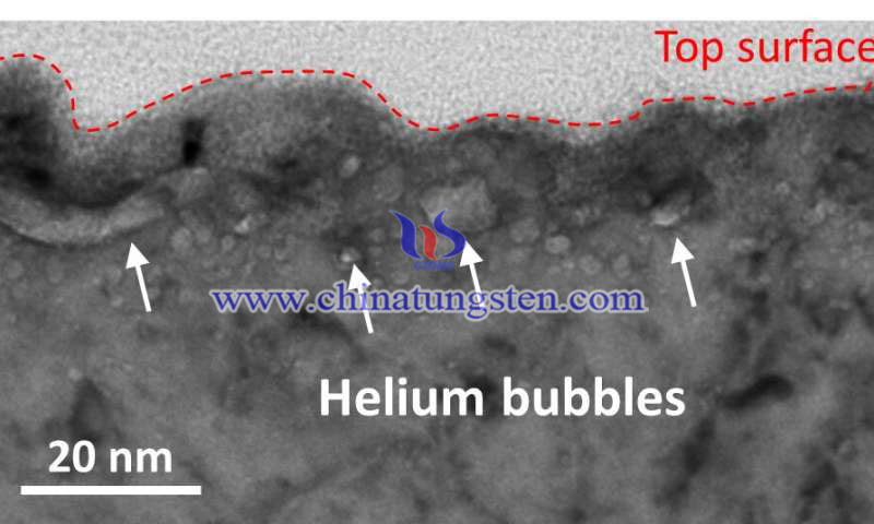
Atomic damage near the top surface of tungsten sample can be clearly identified in the images obtained from TEM observation of the fabricated ultrathin films. Therefore, the "nano-scale sculpture technology" developed by the research team allows cross sections near the top of tungsten samples to be observed at atomic scale. This carving technology can be applied not only to tungsten, but also to other hard materials, such as hardened alloys and ceramics. At present, we are considering the application of this sculpture technology to the automotive industry.
- Tungsten Manufacturer & Supplier, Chinatungsten Online: www.chinatungsten.com
- Tungsten News & Prices of China Tungsten Industry Association: www.ctia.com.cn
- Molybdenum News & Price: news.molybdenum.com.cn
- Tel.: 86 592 5129696; Fax: 86 592 5129797; Email: sales@chinatungsten.com


 sales@chinatungsten.com